Many engineers finish a KiCad design only to hesitate when preparing files for fabrication. Which files belong in the project archive? Which ones must be sent to the manufacturer? Incomplete or incorrect packages cause delays, extra charges, or boards that do not match the design intent. Understanding KiCad's file formats removes that uncertainty and makes the path from schematic to manufactured board predictable.
This article explains the main KiCad file types, what information each one stores, and how they move through the design-to-manufacturing workflow. The focus is practical: what each file does, when it is needed, and which files fabricators actually require.
Why Understanding KiCad File Formats Is Important
KiCad uses open, text-based formats for most design data. This makes projects easy to version-control with Git, simple to share, and resistant to vendor lock-in. At the same time, the number of file types can confuse new users. Knowing the purpose of each format prevents common mistakes such as sending the wrong files to a fabricator, losing library associations, or generating incomplete manufacturing packages.
How KiCad Files Move from Design to Manufacturing
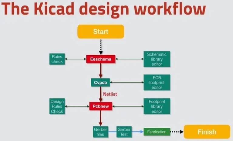
A typical flow looks like this:
- Project and schematic files capture electrical intent.
- The PCB file stores the physical layout.
- Libraries supply the symbols and footprints used in the design.
- After DRC, manufacturing outputs (Gerbers, drill files, BOM, pick-and-place) are generated from the PCB and schematic data.
- The manufacturing package is reviewed and sent to the fabricator.
Each stage produces or consumes specific file types. Keeping the relationships clear ensures the final package accurately represents the finished board.
KiCad Project File Structure
.kicad_pro Project File
The .kicad_pro file is the project definition. It records project settings, the list of schematic sheets, paths to libraries, and other configuration data. Opening a project in the KiCad Project Manager starts from this file. It is small and essential for restoring the complete design environment.
.kicad_sch Schematic File
Each schematic sheet is stored as a .kicad_sch file. Hierarchical designs use multiple sheets linked through the root sheet. These files contain symbols, wires, labels, hierarchical connections, and component fields.
.kicad_pcb PCB Layout File
The .kicad_pcb file holds the complete board: footprints, tracks, vias, copper zones, board outline, layer definitions, design rules, and net information transferred from the schematic. This is the primary file used to generate manufacturing outputs.
A complete project folder typically contains the .kicad_pro, one or more .kicad_sch files, the .kicad_pcb file, and any project-specific libraries.
Schematic Files Explained
Electrical Design Information
The .kicad_sch format stores the logical design. It records every symbol instance, its reference designator, value, footprint association, and custom fields (manufacturer part number, supplier links, etc.). Power symbols, global labels, hierarchical labels, and buses define connectivity across the design.
Components and Connections
Wires and junctions create electrical nets. The file also stores graphical elements, text, and drawing-sheet information used for documentation. Because the format is text-based (S-expression), changes can be tracked in version control and differences reviewed easily.
When the schematic is updated, the “Update PCB from Schematic” command transfers netlist and footprint data into the .kicad_pcb file. Keeping schematic and board synchronized depends on this clean data transfer.
PCB Layout Files Explained
Board Geometry
The .kicad_pcb file defines the board outline, cutouts, mounting holes, and any mechanical features. It also stores the physical placement of every footprint.
Routing Information
Tracks, vias, and copper zones are recorded with their net assignments, widths, and layer locations. Differential pairs, length-tuning data, and net classes are part of the same file.
Layer Settings
Layer stack-up, copper weights (where specified), solder-mask and silkscreen settings, and design-rule constraints live in the PCB file. These settings directly influence the Gerber and drill outputs generated later.
The PCB file is the single source of truth for the physical board. All manufacturing files are derived from it (and from the schematic fields for the BOM).
KiCad Library File Formats
Symbol Libraries (.kicad_sym)
Symbol libraries use the .kicad_sym extension. Each library can contain multiple symbols. Symbols define the graphical representation, pin electrical types, and default fields. Project-specific or global libraries are referenced by the project so the schematic can locate the correct symbols.
Footprint Libraries (.kicad_mod)
Footprints are stored as individual .kicad_mod files inside folders with a .pretty extension. The folder itself acts as the library. Each footprint describes pads, silkscreen, courtyards, fabrication outlines, and 3D model links.
3D Model Files
3D models are typically STEP (.step or .stp) or VRML (.wrl) files. They are referenced by footprints rather than embedded. Accurate 3D models enable mechanical collision checks in the 3D Viewer before manufacturing.
Library files are not usually sent to fabricators, but they are essential for design portability and for regenerating the board if the original project needs to be modified later.
Manufacturing Output Files
Gerber Files
Gerber files (commonly using extensions such as .gbr, or legacy layer-specific names) describe each copper, soldermask, silkscreen, and paste layer as vector data. Modern KiCad generates RS-274X Gerbers that embed aperture information. These files are the primary input for PCB fabrication.
Drill Files
Drill files (usually .drl in Excellon format) list hole locations, sizes, and whether holes are plated or non-plated. Separate files or tool lists may be generated for different drill operations.
BOM Files
The Bill of Materials is typically exported as CSV or spreadsheet format. It lists every component with reference designator, value, footprint, quantity, and any additional fields (manufacturer part number, supplier, etc.) defined in the schematic.
Pick-and-Place Files
Pick-and-place (centroid) files provide X/Y coordinates, rotation, and side of board for every surface-mount component. These files drive automated assembly equipment.
Additional documentation such as assembly drawings or stack-up notes may also be generated, but the four categories above form the core manufacturing package.
Which KiCad Files Should Be Sent to PCB Manufacturers?
Traditionally, fabricators need only the manufacturing outputs, not the native KiCad design files. A complete package usually includes:
- Gerber files for all required layers (copper, soldermask, silkscreen, paste, board outline)
- Drill files (and tool lists if requested)
- BOM (especially if assembly is ordered)
- Pick-and-place file (for SMT assembly)
- A simple README or fabrication notes describing layer stack-up, special requirements, and contact information
Native project files (.kicad_pro, .kicad_sch, .kicad_pcb) and libraries are kept for design archival, version control, and future revisions. They are rarely sent unless specifically requested.
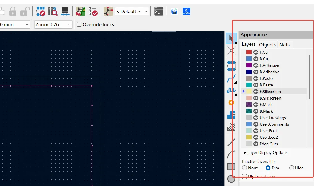
With current KiCad plugin support, the final ordering step can be simplified further. After the design is complete and verified, engineers can use a dedicated plugin button inside KiCad that opens the AIVON PCB quote page directly. The necessary manufacturing data is handled through the plugin workflow, removing the need to manually package and upload Gerber files, drill files, and related outputs. This reduces repetitive file handling and shortens the path from finished layout to order placement on AIVON.
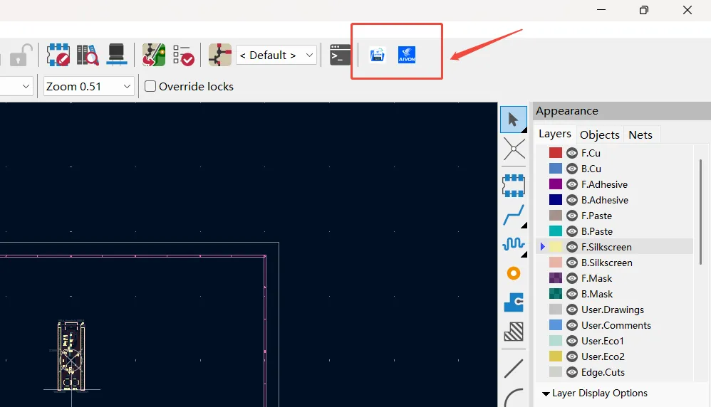
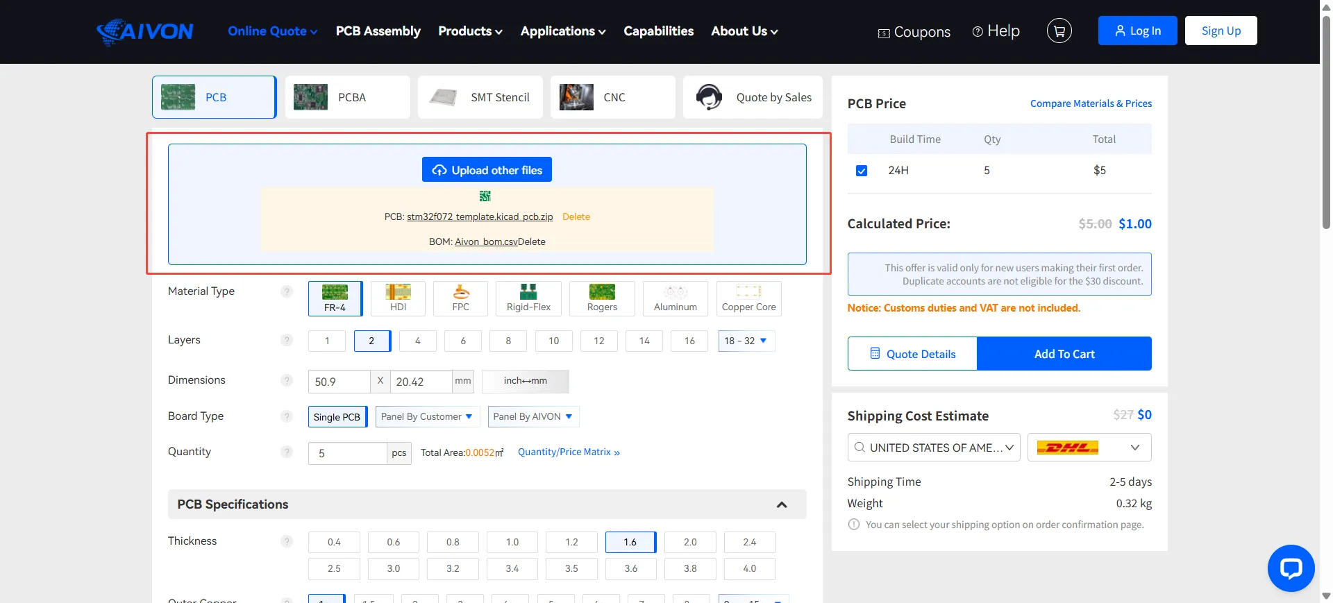
Even when using the plugin route, best practice remains the same: run a full DRC, generate and visually inspect the manufacturing outputs in GerbView, and confirm the board is ready before initiating the order. A clean internal check prevents the majority of fabrication issues regardless of how the files are ultimately submitted.
Understanding KiCad file formats turns an opaque collection of files into a logical pipeline. The project, schematic, and PCB files capture design intent; libraries provide reusable elements; manufacturing outputs translate that intent into data the fabricator can use. Whether the final submission is a traditional file package or a streamlined plugin-based order through AIVON, mastering these formats reduces errors, simplifies collaboration, and ensures that the boards you receive match the design you created.
FAQ
Q1: What is the difference between .kicad_sch and .kicad_pcb files?
A1: The .kicad_sch file stores the electrical schematic (symbols, wires, nets). The .kicad_pcb file stores the physical board layout (footprints, tracks, zones, layers). Data moves from schematic to board via the update command.
Q2: Do I need to send .kicad_pro or library files to the PCB manufacturer?
A2: No. Manufacturers need Gerber, drill, BOM, and pick-and-place files. Native KiCad project and library files are for design work and archival.
Q3: What format are modern KiCad Gerber files?
A3: KiCad generates RS-274X Gerbers that embed aperture definitions. This is the standard format accepted by virtually all PCB fabricators.
Q4: Where are footprints stored in KiCad?
A4: Footprints are individual .kicad_mod files collected inside folders that end with .pretty. The folder acts as the footprint library.
Q5: Why should I keep the original KiCad project files after ordering boards?
A5: The native files allow future revisions, library updates, and design reuse. Manufacturing outputs are a snapshot for fabrication; the project files remain the editable source of truth.