Many engineers generate Gerber files the moment DRC shows zero errors and immediately upload them for fabrication. Days later the manufacturer returns a DFM report listing missing layers, incorrect drill sizes, copper too close to the edge, or footprints that cannot be assembled. Each of these issues costs time and money that could have been avoided with a short, systematic check before ordering.
This checklist covers the ten essential items every KiCad user should verify before placing a PCB order. Following it converts a design that merely "passes DRC" into a package that is ready for real production.
1. Confirm Layer Count and Stack-up
Open Board Setup and verify that the number of copper layers matches what you intend to order. Add a clear stack-up note (copper weight, dielectric type, overall thickness, surface finish) so the manufacturer does not have to guess. Mismatched layer count is one of the fastest ways to receive the wrong boards.
2. Check Board Dimensions and Outline
Measure the board outline on the Edge.Cuts layer. Confirm that the dimensions match the mechanical drawing and that the outline is a single closed shape. Leave the manufacturer's required copper-to-edge clearance (typically 0.3–0.5 mm). Incorrect outline data causes panelization problems and dimension rejects.
3. Verify Copper Thickness
Confirm the copper weight (usually 1 oz or 35 µm for outer layers) in your design notes and in the manufacturer's order form. High-current designs may need heavier copper; controlled-impedance designs need the exact weight used in the stack-up calculation. Ordering the wrong copper weight changes both electrical performance and cost.
4. Review Drill Sizes and Via Specifications
Export the drill report and check every hole size against the manufacturer's minimum drill and aspect-ratio limits. Confirm that via annular rings meet the fab's requirement (commonly ≥ 0.125 mm). Non-plated holes, slots, and back-drills must be clearly identified. Unsupported drill sizes are a frequent cause of DFM rejection.
5. Confirm Footprints and Land Patterns
Spot-check every unique footprint against the component datasheet land-pattern recommendation. Verify pad sizes, thermal pads, polarity marks, and courtyards. Incorrect footprints pass electrical DRC yet fail at assembly. This single check prevents many soldering and inspection problems.
6. Run DRC with Manufacturing Rules
Load design rules that match the target manufacturer's capabilities (trace width, clearance, via size, copper-to-edge). Run a full Design Rule Check and clear every error and relevant warning. A clean result against optimistic rules is meaningless; a clean result against real process limits is the best predictor of DFM success.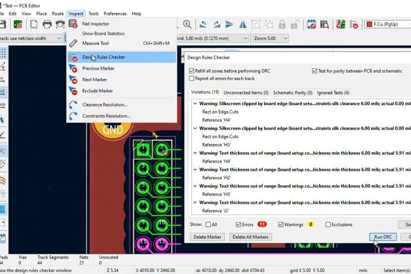
7. Generate Correct Gerber and Drill Files
Plot Gerbers for all required layers (copper, solder mask, silkscreen, board outline) using the correct format (usually RS-274X). Generate Excellon drill files for plated and non-plated holes. Open the entire set in a Gerber viewer and confirm that no layers are missing or misaligned. File-format or naming mistakes still cause order delays.
8. Check Silkscreen and Solder Mask
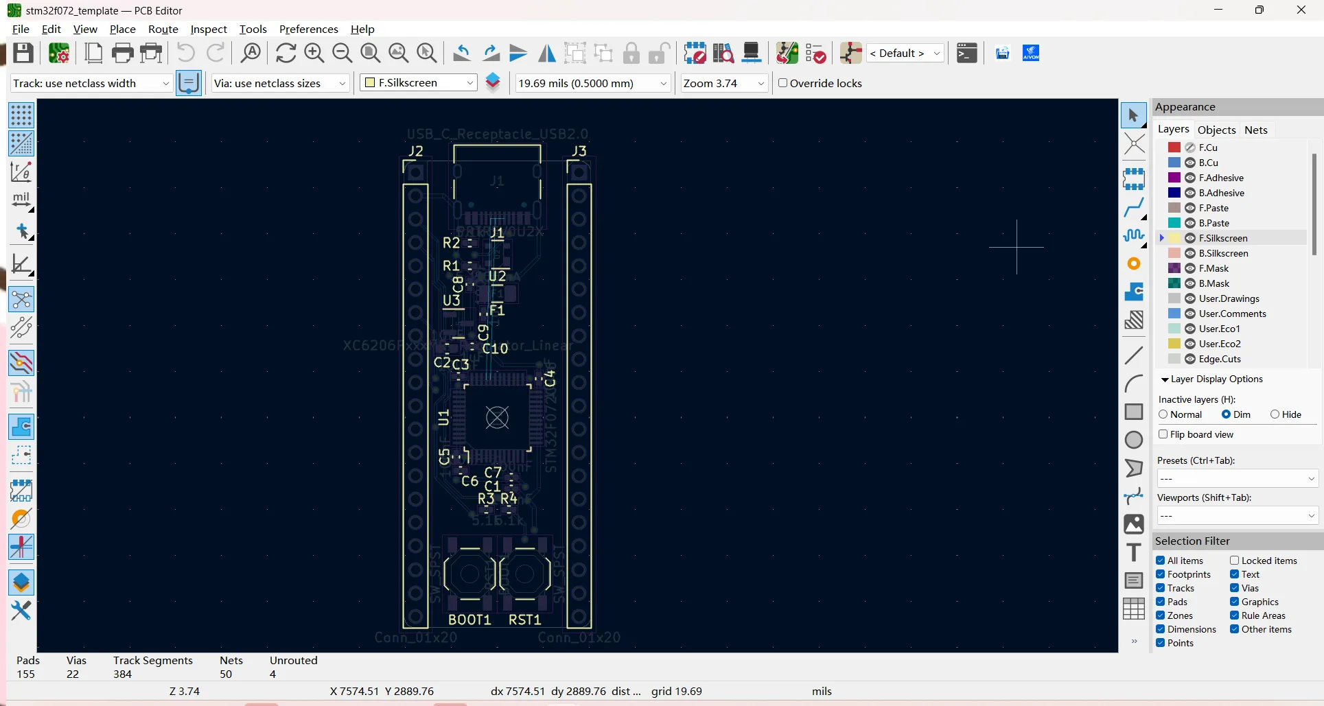
Ensure reference designators are readable and do not overlap pads or vias. Confirm that polarity marks and pin-1 indicators are present. Verify solder-mask openings are correct and that minimum solder-mask dam requirements are met. Silkscreen or mask errors are cosmetic on screen but create real assembly and inspection issues.
9. Prepare BOM and Pick-and-Place Files
Export a BOM that includes manufacturer part numbers, quantities, and reference designators. Generate a pick-and-place (centroid) file and verify that coordinates and rotations match the silkscreen. Incomplete or mismatched assembly data forces the assembler to stop and ask questions.
10. Perform Final Visual and 3D Review
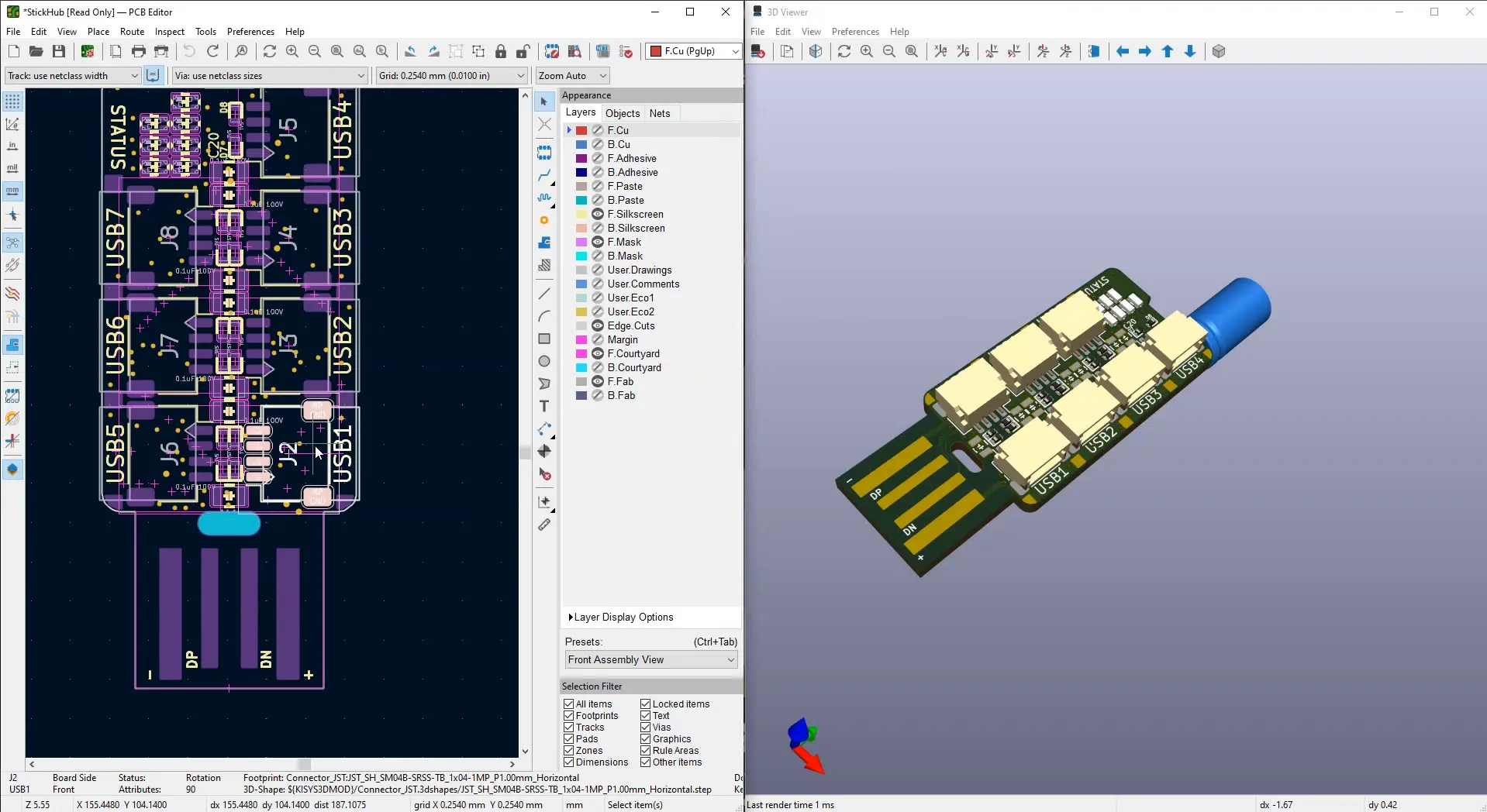
Inspect the board in both 2D and 3D viewers. Look for component collisions, insufficient keep-outs, unbalanced copper, and any remaining DRC warnings. A five-minute visual pass often catches problems that automated checks miss.
How AIVON Helps Validate KiCad Designs Before Production
After the ten checks above are complete, the remaining risk is that the files still contain subtle issues only a manufacturing engineer would notice. AIVON's engineering team reviews KiCad-originated designs against real process capabilities before production begins. When you use the AIVON KiCad plugin, the design data moves directly from your project into quotation and engineering review without manual re-packaging. This preserves accuracy, surfaces DFM comments early, and shortens the path from verified layout to ordered boards.
A short, disciplined checklist performed in KiCad before you click "order" is the highest-leverage step you can take to avoid manufacturing problems. Confirm the stack-up, dimensions, copper, drills, footprints, rules, Gerbers, silkscreen, assembly data, and final appearance—then submit a package that is truly ready for production.
FAQ
Q1: What should I check in KiCad before ordering a PCB?
A1: Verify layer count and stack-up, board dimensions, copper thickness, drill sizes, footprints, DRC results against manufacturing rules, Gerber and drill files, silkscreen/solder mask, BOM and pick-and-place data, and perform a final visual/3D review.
Q2: Why does my KiCad board pass DRC but still have manufacturing problems?
A2: Local DRC only checks the rules you loaded. If those rules are looser than the manufacturer's process limits, or if Gerbers, drills, or footprints contain errors, the fab's DFM review will reject the job. Always use factory-matched rules and inspect the actual manufacturing files.
Q3: How do I make sure Gerber files are correct before ordering?
A3: Generate all required layers and Excellon drills, then open the complete set in a Gerber viewer. Confirm every layer is present, aligned, and free of obvious defects before uploading.
Q4: What is the most common checklist item that engineers skip?
A4: Footprint verification and final visual/3D inspection are frequently skipped. Both catch problems that pure electrical DRC cannot detect and that cause assembly failures.
Q5: When is the best time to run this manufacturing checklist in KiCad?
A5: Run the full checklist after the board has passed DRC with manufacturing-aware rules and immediately before generating the final Gerber package for ordering.
```