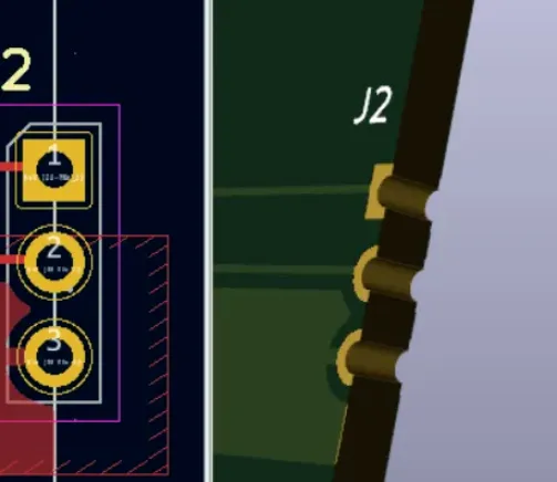
New users often open KiCad and encounter multiple windows, toolbars, and panels without a clear map of how they fit together. The software separates tasks into dedicated workspaces so each stage of design stays focused, yet that modular structure only becomes efficient once the overall organization is understood. Knowing which window does what—and how data moves between them—reduces friction and helps engineers produce clean manufacturing files on the first attempt.
This article explains the KiCad interface structure, the role of every major workspace, and the relationships that connect them. The emphasis is on orientation and navigation so beginners can move confidently through a complete project.
Overview of KiCad Interface and Project Workflow
KiCad is built around a single project folder. All schematic sheets, the board file, libraries, and output files belong to that project and are coordinated from one central location. Designers do not work inside a single all-in-one window; instead they move between specialized editors as the design progresses from connectivity definition to physical layout and finally to fabrication data.
Understanding the workspaces improves efficiency because every command, panel, and check has a logical home. Once the map is clear, time is spent on electrical and manufacturing decisions rather than searching for tools. The same structure also supports the full engineering sequence: design, verification, manufacturing-file generation, DFM review, fabrication, and assembly.
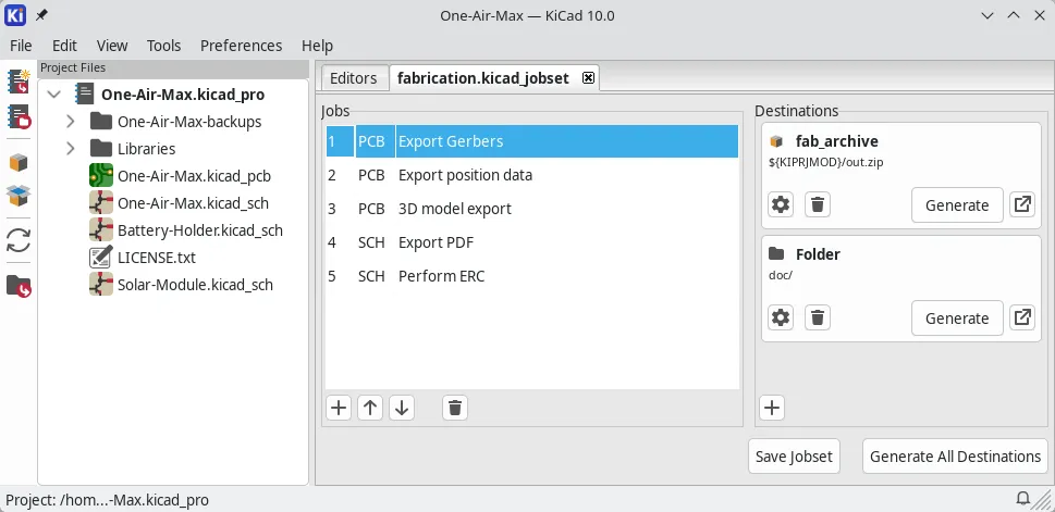
KiCad Project Environment Overview
Project Manager
The Project Manager is the starting point and permanent reference for any KiCad project. It displays the complete project tree—schematic files, PCB file, associated libraries, and generated outputs—and provides the buttons that launch every major editor. From this window you create or open projects, archive the full set of files, and access global preferences.
Keeping the Project Manager visible (or easily accessible) helps beginners maintain context. It is the place to return whenever the relationship between files needs to be checked or another editor needs to be opened.
Relationship Between Different KiCad Editors
KiCad uses a clear modular architecture:
- The Schematic Editor defines electrical connectivity and prepares footprint information.
- The PCB Editor receives that information and creates the physical board.
- Symbol and Footprint Editors maintain the reusable library elements used by the other two.
- Visualization and verification tools confirm the design before files are released for manufacturing.
Data flows primarily from schematic to board through a dedicated update command. Cross-probing works in both directions, so selecting a net or component in one editor highlights the corresponding item in the other. This linkage keeps schematic and layout synchronized and reduces the risk of mismatches that later appear as assembly or fabrication problems.
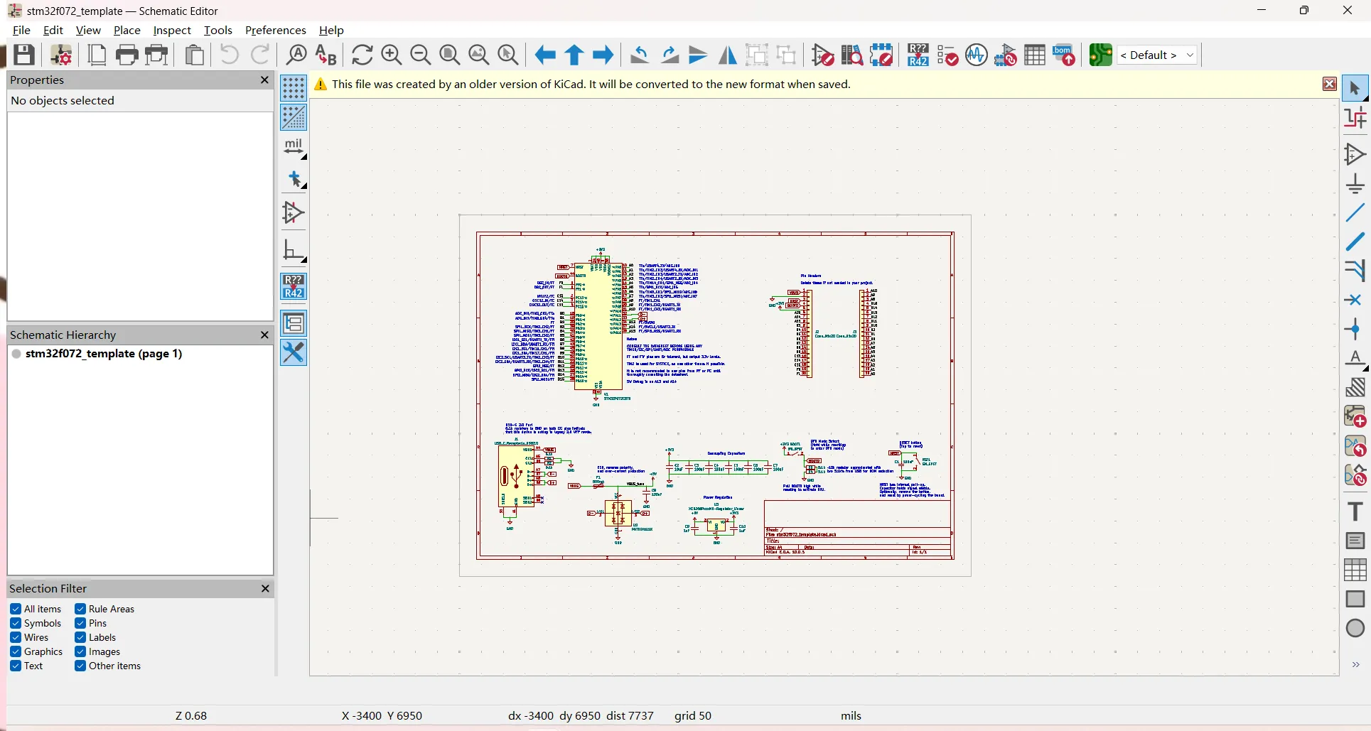
Schematic Editor Explained
The Schematic Editor is the workspace for capturing the electrical design. It is the natural starting point for a new project and the place where hierarchical organization, symbol placement, and connectivity are established.
Sheets can be single-page or hierarchical. Hierarchical organization keeps larger designs readable and reusable. Symbols are placed, wires and buses create connections, and labels manage nets across sheets. Reference designators and footprint associations are handled here so the later board update carries complete information. Electrical Rules Check runs inside this editor and should be completed before any data is transferred to the PCB.
The Schematic Editor's panels—hierarchy navigator, net navigator, and properties—support navigation and inspection on multi-sheet designs. Once the electrical intent is stable and verified, the design is ready to move forward.
PCB Editor Explained
The PCB Editor is the physical-layout workspace. It receives the netlist and footprints from the schematic and turns them into copper, silkscreen, solder mask, and mechanical layers.
PCB Layout Workspace
Footprints appear after the update from schematic. The board outline is defined, components are arranged, and routing begins. The properties panel, selection filters, and appearance controls help manage density as the board grows.
Layer Management
The Layers Manager is one of the most important panels in this workspace. It controls visibility and ordering of copper layers, technical layers (mask, paste, silkscreen), and user-defined layers. Correct layer understanding is essential for both design clarity and accurate manufacturing-file generation.
Routing and Design Rule Control
Board Setup contains the layer stack, design rules, and net classes. These settings should be established early. The interactive router and copper-zone tools operate under those rules. Design Rule Check runs inside the PCB Editor and is the primary verification step before manufacturing outputs are created.
Symbol and Footprint Editors
The Symbol Editor and Footprint Editor are library-focused workspaces. They are not required for every simple project that relies only on official libraries, yet they become essential when a missing or custom part is needed.
The Symbol Editor creates or adjusts the graphical and electrical representation used in the schematic. The Footprint Editor defines the physical land pattern that will appear on the board and be used by the assembler. Both editors manage libraries that can be project-specific, personal, or shared across a team. Consistent library practice keeps designs portable and reduces errors when the same parts reappear in later projects.
Visualization and Verification Tools
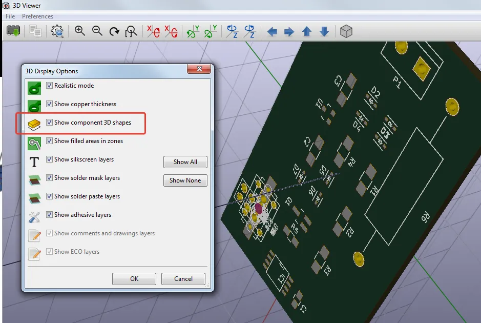
3D Viewer
The 3D Viewer provides a realistic rendering of the finished board with component models. It is the practical place to evaluate mechanical fit, connector clearances, and overall height before any physical prototype is ordered.
Gerber Viewer
GerbView loads the Gerber and drill files produced by the PCB Editor. It allows a final inspection of the exact data that will be sent to the fabricator, confirming layer alignment and completeness.
Design Rule Check (DRC)
DRC examines the board against the rules defined in Board Setup. A clean result is the internal signal that the design is ready for manufacturing-file generation.
These three tools close the verification loop after layout is complete and before files leave the design environment.
How Beginners Should Navigate KiCad
A simple, repeatable navigation pattern helps new users stay oriented:
- Begin every project in the Project Manager so the full file structure is visible.
- Complete and verify the schematic before opening the PCB Editor.
- Use the official update command to transfer data from schematic to board.
- Establish board setup (layers and rules) early in the PCB Editor.
- Work iteratively between routing and verification tools.
- Inspect the design in the 3D Viewer and the generated files in GerbView.
- Only after these checks generate the final manufacturing package.
Following this sequence keeps the relationship between workspaces clear and prevents the most common orientation problems. Once the map is familiar, attention shifts from locating commands to making the engineering decisions that affect performance and manufacturability.
When the design is fully verified, the manufacturing files can be exported and submitted for fabrication. Engineers routinely send the Gerber, drill, BOM, and pick-and-place outputs produced by KiCad to services such as AIVON for PCB fabrication and assembly. Because the files follow industry standards, the handoff remains straightforward after the internal interface checks have been completed.
Understanding every workspace turns KiCad into a predictable environment. The Project Manager provides the organizing view, the Schematic and PCB Editors handle the core design stages, the library editors maintain reusable elements, and the visualization tools confirm readiness for manufacturing. Mastering this structure is the fastest way for beginners to move from first schematic to reliable boards.
FAQ
Q1: Which window should I open first when starting a new KiCad project?
A1: Always start in the Project Manager. It shows the complete project structure and provides the launch buttons for every other workspace.
Q2: How are the Schematic Editor and PCB Editor connected?
A2: Data moves from schematic to board through the “Update PCB from Schematic” command. Cross-probing also works in both directions so selections in one editor highlight the corresponding items in the other.
Q3: Do beginners need to use the Symbol and Footprint Editors immediately?
A3: Not for the first simple projects that rely on official libraries. These editors become important when a required part is missing or a custom package is needed.
Q4: What is the difference between the 3D Viewer and Gerber Viewer?
A4: The 3D Viewer shows a realistic model of the finished board for mechanical checks. Gerber Viewer displays the exact fabrication files that will be sent to the manufacturer.
Q5: What is a reliable navigation order for a complete KiCad project?
A5: Project Manager → Schematic Editor (with verification) → update to PCB Editor → layout and rules → 3D Viewer and DRC → generate files → Gerber Viewer. Completing each stage before moving forward keeps the design coherent and manufacturing-ready.