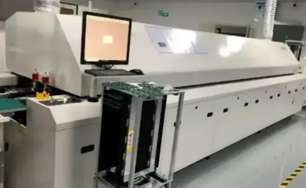
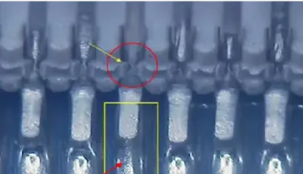
Ball Grid Array (BGA) is an advanced surface-mount packaging technology that replaces traditional peripheral leads with an array of miniature solder balls on the underside of the package. These solder balls provide the electrical and mechanical connection between the device and the printed circuit board (PCB). While BGAs enable high I/O density and improved electrical performance, a range of soldering defects can occur during reflow. This article summarizes the most common BGA reflow defects, how to detect them, typical root causes, and practical process improvements based on shop-floor experience.
Solder Bridging
Solder bridging occurs when two or more adjacent joints are unintentionally connected by solder. This defect is unacceptable because it creates electrical shorts. Post-reflow inspection should include electrical test, optical inspection with a borescope, and X-ray to identify and locate bridges.
Common causes include poor solder paste printing, placement offset, handling-induced disturbance of the placed component, solder spatter during reflow, and oversized solder balls. Corrective actions should target these root causes: raise stencil printing quality, fix print-related issues, correct placement coordinates, and optimize the reflow profile.
Cold Solder Joints
A cold solder joint results when the paste does not fully reflow. These joints are unacceptable because inadequate wetting and incomplete metallurgical bonding reduce mechanical integrity and can cause electrical failure or intermittent functionality.
Root causes include insufficient reflow temperature (failing to exceed the solder alloy's liquidus) and poor wetting on the pad or ball surface. Cross-sectioning and microscopic examination are effective ways to confirm this defect.
Open Circuits
An open joint breaks the electrical continuity and is unacceptable. Opens are commonly detected by electrical testing, borescope inspection, and X-ray.
Typical causes include solder paste print defects, placement misalignment, component coplanarity issues, PCB solderability problems, and excessive mechanical stress that cracks the joint over time. Any of these can lead to partial or complete opens.
Insufficient or Uneven Heating
Insufficient or non-uniform heating of a BGA during reflow is a common process issue, and it is frequently seen during rework. Several factors can cause this behavior:
- Multilayer boards with large ground and power planes, which act as heat sinks.
- Double-sided assemblies where shielding components on the opposite side sit underneath or near the BGA location.
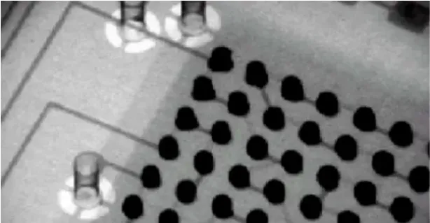
- High-conductivity structures that draw heat away from the BGA during reflow. A typical X-ray signature is varying solder ball sizes across the package footprint.
On X-ray, insufficient heating often appears as partially unsoldered balls under the center or on one side of the package. Affected balls may have rough surfaces, indicating partial reflow and inadequate time for full pad wetting and collapse. Ball offset or elongation is another sign of insufficient heating. Oblique X-ray imaging at approximately 45° is useful to localize areas with poor heating or wetting. A properly formed joint has a solder ball that fully wets the pad and forms a smooth columnar connection. Inadequate heating shows incomplete pad wetting or an elongated ball image, indicating the ball and paste did not merge into a single joint.
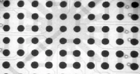
Figure 1 | X-ray image showing non-uniform heating—balls at the bottom appear larger than those at the top.
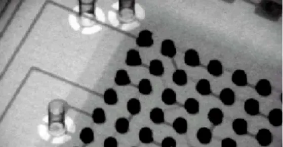
Figure 2 | 45° oblique X-ray reveals insufficient heating in one corner. The top image shows irregular solder joint shapes.
Head-in-Pillow (HoP)
Head-in-pillow (HoP) is characterized by a visible interface between the partially collapsed BGA ball and the solder paste reflowed on the PCB pad. Part of the joint forms from the original ball, part from the PCB paste, but they fail to fully coalesce. HoP is also known as head and pillow, head in pillow, ball in cup, ball in socket, or hidden pillow.
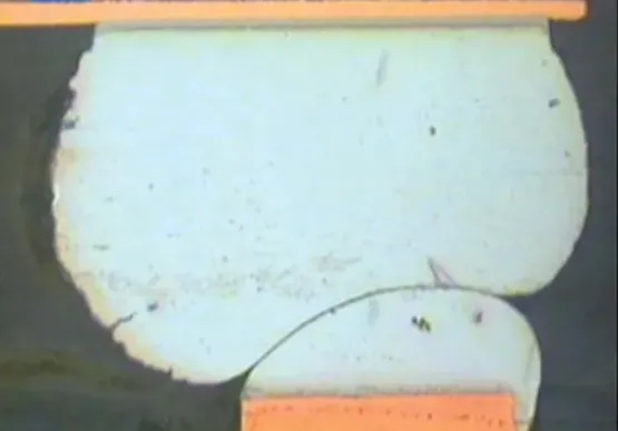
Figure 3 | Head-in-pillow schematic. The solder ball and paste do not merge.
The formation sequence is illustrated below. The BGA is placed on the PCB pads with printed paste. As temperature rises in the reflow oven, dynamic warpage of the package and PCB may increase the gap between the ball and paste. The solder on the PCB pad melts and becomes covered with flux. The solder ball also begins to melt, but with little or no flux coverage, its surface oxidizes. When the BGA collapses, the ball recontacts the molten paste. Ideally the two merge to form a sound joint. If flux activity is insufficient or oxidation on the ball surface is excessive, HoP results.
Dynamic Warpage
During reflow, coefficient of thermal expansion (CTE) mismatch between the package substrate and silicon die causes the package to warp as temperature increases. This can lift some balls off the printed paste. Flux remains on the PCB pad while the lifted balls, starved of flux, oxidize. HoP often occurs at the peak of warpage, and adjacent joints may appear elongated.
Severe package corner warpage is a typical driver of HoP, especially when a thin PCB bends or sags in reflow without mechanical support. When board or package warpage dominates, many balls can show HoP-like signatures, and adjacent joints may be stretched.
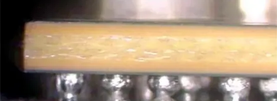
Figure 4 | Head-in-pillow caused by severe package warpage at a corner.
Reflow Profile and Liquidus Time Delay
Reflow profile parameters strongly influence HoP due to temperature gradients (delta-T, dT). Board copper distribution, laminate and package materials, and BGA type and size all contribute to dT, which can exist within a single component. Airflow effects also create dT between the outer and inner rows of balls. Outer rows typically reach higher temperatures earlier than inner rows, delaying inner-row melting. Collapse occurs only after inner rows melt; until then, outer rows can be exposed to high temperature without flux protection, promoting oxidation and HoP.
The difference in the time each row spends above the liquidus is the liquidus time delay (LTD), which is a critical factor in HoP.
To minimize HoP, ensure actual time-above-liquidus (TAL) is long enough after collapse to form a sound joint across all rows.
Solder Paste Characteristics
Under lead-free reflow temperatures and temporary ball–paste separation, paste chemistry is critical. The flux must maintain activity at high temperature to prevent oxidation. Three key properties affecting HoP are: stability with respect to time and temperature, wetting performance, and oxidation resistance. Poor oxidation resistance allows the graping phenomenon, where unmelted solder particles remain after reflow.
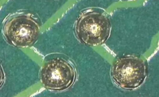
Figure 5 | Unmelted solder particles after reflow indicating poor oxidation resistance of the paste.
How to Reduce HoP
HoP is multifactorial and often driven by multiple failure modes simultaneously. The most effective approach is to identify and address the dominant contributors.
- Increase solder paste volume uniformly across all BGA pads to reduce HoP incidence.
- Tune the reflow profile: increasing TAL and peak temperature can reduce HoP by extending the post-collapse contact time between balls and molten paste. Soak time also influences HoP, depending on paste chemistry. Follow paste supplier guidance and avoid pre-reflow conditions that squeeze out or dry the flux.
- Reflow in nitrogen to reduce oxidation and improve yield.
Non-Wet Open (NWO) / Floating Solder Ball
A defect closely related to HoP is the non-wet open (NWO), sometimes called a floating solder ball. This typically occurs with severe BGA warpage. During reflow, paste detaches from the pad and adheres to the lifted ball. As the gap forms and the solder fuses to the ball instead of the pad, the pad surface remains at high temperature without flux protection, allowing oxides to build. The result is an open joint on the PCB pad, with no intermetallic compound (IMC) formed. The pad may appear as if no paste was printed.
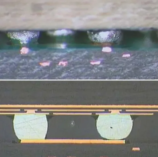
Figure 6 | Example of a floating solder ball/non-wet open.
Factors influencing NWO include solder paste and flux type, PCB pad surface finish (such as OSP), pad design (solder mask defined vs. non-solder mask defined), and internal copper planes that conduct heat. Mitigations mirror those for HoP: adjust paste chemistry, increase paste volume, and use nitrogen. Increasing BGA pad size can also help by creating a larger paste area and stronger surface-tension forces that retain solder on the pad rather than allowing the ball to pull it away.
Component-Related Defects
Improper handling and storage before reflow can cause component defects such as the popcorn effect and BGA package warpage. Each has characteristic X-ray signatures.
The popcorn effect causes swelling under the die area, pushing the central balls outward and flattening them between the package and the PCB. This can enlarge central joints and even cause bridging.
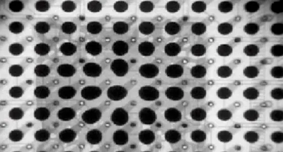
Figure 7 | X-ray signature of the popcorn effect with enlarged central balls.
Package warpage is harder to spot than the popcorn effect. Warpage is usually greatest at the package corners, where X-ray often shows elongated joints. Optical microscopy can corroborate these findings. Stress relief during reflow may also leave visible ripples on the package substrate.
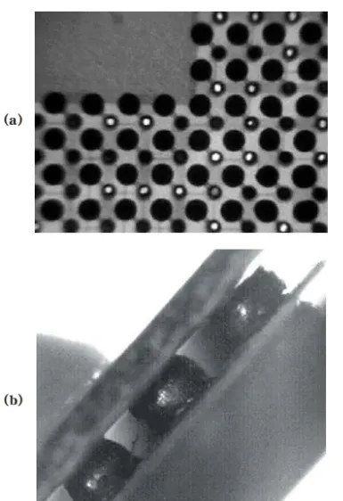
Figure 8 | BGA warpage: (a) X-ray shows elongated joints at the lower right corner, (b) optical view shows warpage with the ball top pulled away from the package and substrate ripples from stress relief.
Inspection, Correlation, and Process Improvement
Inspection data is essential for controlling manufacturing processes and maximizing quality and yield. Every assembled component carries process information—acceptable or not—that can be observed through inspection. Visual checks often provide the earliest clue: examine all four edges of the BGA. The standoff height should be uniform, and the perimeter ball shapes should appear consistent.
To directly evaluate joints beneath the BGA, use X-ray or borescope inspection. These methods detect obvious defects like bridging or missing balls and are also useful for characterizing reflow quality. Check for uniformity in ball size and shape. Properly collapsed balls increase in size compared to their pre-reflow diameter. For example, a PBGA with 0.75 mm balls may exhibit post-reflow diameters around 0.90 mm—about a 20% increase. From the package center to its edges, ball area variation of about 10–15% is typical; significantly larger variation indicates process issues. In contrast, poorly wetted balls tend to remain round and nearly uniform across the package.
Oblique-angle X-ray is particularly useful for assessing the solder-to-pad contact region. By tilting the sample, the pad-to-ball interface is no longer shadowed, allowing the operator to verify pad contact and complete wetting.
Quantitative X-ray image analysis using software can detect subtle changes in joint size and shape that are difficult to see by eye. While not strictly necessary for BGA inspection, these tools can reveal small process signatures associated with known failure modes, enabling proactive monitoring and timely corrective action.