In many SMT lines, attention often goes to 0201 and 01005 miniature components, while the process evolution for through-hole components is overlooked. Traditional wave soldering is increasingly being replaced by pin-in-paste (PIP) reflow.
PIP eliminates the wave solder step, enables true SMT mixed assembly, and significantly improves throughput. The prerequisite, however, is disciplined pad and hole design. This article details the PCB layout and pad rules that make PIP reliable in production.
1. Core Logic of the PIP Process
The essence of PIP is to print solder paste into plated through holes (PTH), place the through-hole components, and then complete all solder joints in a single reflow cycle. Achieving robust solder joints requires targeted adjustments in PCB layout, including:
-
Single-side placement: Place all through-hole (THT) components on the same side of the PCB to avoid stencil and paste-printing interference.
-
Pin-to-hole ratio (PH): The key parameter that governs solder volume and through-hole fill.
-
Shape matching: The pin geometry must match the plated hole geometry to ensure adequate paste retention and capillary action.
2. Precise Sizing of Pins and Hole Diameters
If the pin is too small relative to the hole, solder paste will drain through the barrel before reflow. If the hole is too tight, paste cannot fill the barrel and the solder volume will be insufficient. Pin and hole sizing therefore requires quantitative design.
2.1 PH (Pin-to-Hole) Ratio
PH is the primary indicator of how well a pin fits the hole for PIP soldering. The formula is shown below.
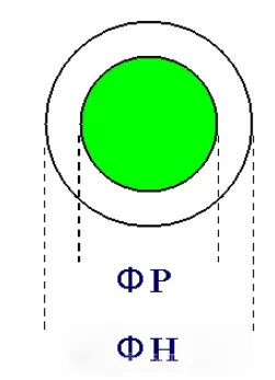
Based on the PH value, expected solderability can be categorized as follows:
| PH range | Assessment | Notes |
|---|---|---|
| 0.6–0.8 | Better | High joint strength and ideal through-hole fill. Preferred design. |
| 0.4–0.5 | Acceptable | Usable with caution. Closely manage stencil aperture and paste volume. |
| < 0.4 | Poor | Prone to insufficient wetting and opens. Not recommended. |
2.2 Matching Pin Shapes to Hole Geometry
Pin geometry dictates the hole geometry. Match them carefully and observe the following constraints during PCB library and footprint design:
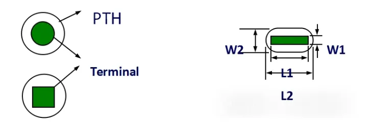
| Pin shape | Hole type | Design rule |
|---|---|---|
| Round / Square | Round hole | Area ratio: A(P) ÷ A(H) ≤ 0.5 (i.e., the pin cross-sectional area should not exceed 50% of the hole area). |
| Rectangular | Oval hole |
Aspect ratio: L2:W2 ≥ 1.5:1 Dimensional allowances: L2 ≈ L1 + 0.4 mm; W2 ≈ W1 + 0.4 mm |
Explanation: For rectangular leads, an oval hole with an aspect ratio above 1.5:1 provides sufficient clearance around the pin to retain solder paste and promote capillary flow during reflow.
3. Mandatory Layout Rules
Beyond dimensional fit, spatial planning is critical for robust paste printing and reflow.
-
Solder paste printing keepout: The component courtyard defines the paste printing keepout for PIP components. Do not place other components within this courtyard to avoid blocking stencil access and squeegee travel.
-
Solder mask dams for isolation: If any PTH annular ring connects to an adjacent connector pad, you must add a solder mask dam at least 20 mil wide between them to prevent bridging during reflow.

-
Safety clearance: To accommodate the larger solder paste deposits used in PIP, keep at least 2.5 mm clearance between PTH holes and neighboring SMT pads.

4. Special Mechanical Features: Board Locks and Guide Pins
For mechanical retention features such as board locks and guide pins, design targets are adequate mechanical strength and controlled insertion force. The connector must be firmly anchored without risking placement or reflow issues. Pay attention to the following:
4.1 Board Lock / Kink Design
These features secure the connector to the PCB and resist loosening.
| Item | Design requirement |
|---|---|
| Hole selection | Use oval holes matched to the kink (barbed) feature of the pin. |
| Aspect ratio | Oval hole aspect ratio must satisfy L:W > 1.5:1. |
| Insertion force | Insertion force into the PCB should be ≤ 2.5 kg. |
| Stability | No tilt, rocking, or tendency to loosen after insertion. |
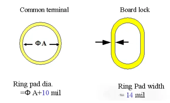
| Pad design | Annular ring width = 14 mil. |
4.2 Boss / Guide Pin Design
Guide features are used to locate large connectors during placement.
| Item | Design requirement |
|---|---|
| Hole fit | Maintain insertion force ≤ 2.5 kg. |
| Pad design | Annular ring diameter = ΦA + 10 mil, where ΦA is the finished hole diameter. |
5. Summary
PIP is highly efficient, but it raises the bar for DFM. Keep these rules front and center:
-
Tune the PH ratio: Aim for 0.6–0.8 to balance paste retention, wetting, and through-hole fill.
-
Match shapes correctly: Rectangular leads with oval holes; round or square pins with round holes. Observe the area and aspect-ratio constraints.
-
Provide adequate spacing: Maintain 2.5 mm clearance to adjacent pads and use 20 mil solder mask dams where needed.
With disciplined pin/hole sizing, correct hole geometry, and sound layout keepouts, PIP can deliver robust through-hole joints within a standard SMT reflow process, eliminating secondary soldering while preserving joint reliability.