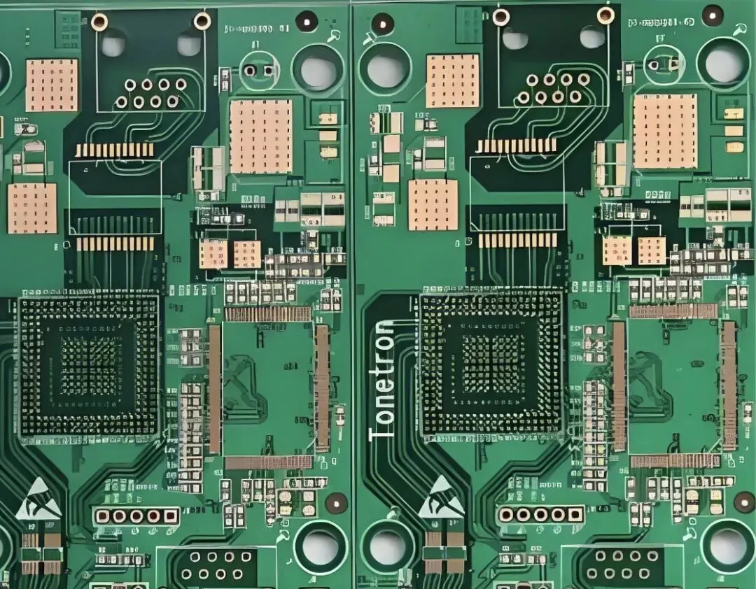
On an SMT production line, registration is the lifeline of quality. For ICs we rely on fiducial marks, while for connectors we rely on plastic locating pins. Yet many designers still draw the PCB's non-plated through holes (NPTH) for these plastic posts to be exactly the same diameter as the locating pins. That "just fits" approach is a major mistake.
This article explains a fundamental design-for-manufacturing rule: for SMT connectors, non-soldered plastic locating pins must be strictly smaller than the PCB's molded NPTH holes to ensure a true clearance fit—no interference, no friction, and no insertion force—after all dimensional tolerances are considered.
1. The Rule at a Glance: Always Use a Clearance Fit
Core requirement:
To support automated placement, the plastic locating pins on an SMT connector that are not intended to be soldered must be smaller than the NPTH registration holes, with sufficient clearance to guarantee zero interference under worst-case tolerance conditions.
Plain-language interpretation:
- Subject: Plastic locating posts on the bottom of the connector (non-soldered features).
- Mating feature: Non-plated through holes (NPTH) on the PCB.
- Fit relationship: The hole must be clearly larger than the pin.
- Goal: No rubbing, no press-fit behavior, and no chance of jamming.
2. Why "Just Fits" Becomes a Disaster
A common misconception is "If the pin can go in, it's fine." In reality, pick-and-place machines impose stringent requirements on verticality and coplanarity, and the manufacturing system always includes dimensional variation. Designing for a zero-gap fit ignores how these variations combine.
2.1 Tolerance Stack-Up
This is the core reason to avoid a tight fit. Real production parts never match their nominal dimensions exactly. Multiple sources of variation can stack up in unfortunate combinations:
| Error Source | Impact |
|---|---|
| PCB drilling tolerance | The NPTH may be off-position or undersized (typically ±0.05 mm to ±0.1 mm). |
| Connector molding tolerance | The plastic locating pin may be eccentric or slightly oversized. |
| Pick-and-place accuracy | Component pickup and placement can introduce about ±0.05 mm of placement error. |
The result: If the design targets a zero-clearance fit, any small combination of these errors can prevent the pin from entering the hole at all. On the line, that translates directly to open solder joints or excessive standoff because the connector cannot sit flat.
2.2 Avoid "False Placement" and Stress Concentration
If the pin and hole are designed as an interference fit:
- Forced insertion: The placement nozzle may push down with high force to seat the part, potentially cracking the plastic or damaging the nozzle.
- Residual stress: Even if forced in, significant elastic stress remains trapped in the connector body. During reflow, as the plastic softens, that stress is released, causing the connector to lift or skew, degrading coplanarity and joint integrity.
3. Visualizing Correct vs. Incorrect Fit
Consider two contrasting designs:
Incorrect Design (Interference Fit)
Connector pin (diameter 1.00 mm)
        │
        ▼
[ PCB NPTH hole (diameter 1.00 mm) ]
- Condition: Tight fit with friction.
- Consequence: Placement alarms, inability to place, or damage to the nozzle/component.
Correct Design (Clearance Fit)
Connector pin (diameter 1.00 mm)
        │
        ▼
[ PCB NPTH hole (diameter 1.20 mm–1.30 mm) ]
- Condition: Clearance fit with noticeable free play for the pin inside the hole.
- Consequence: Easy placement. During reflow, solder surface tension pulls the connector into final alignment.

4. DFM Checklist for Connector Locating Pins
Use this three-step process to ensure robust connector registration and high assembly yield.
4.1 Consult the Datasheet
- Always consult the connector's datasheet before footprint design.
- Pay attention to: The recommended PCB layout (pad and hole pattern).
- Confirm: The datasheet's NPTH diameter for plastic locating pins is typically 0.2–0.5 mm larger than the actual pin diameter. Use these values as provided.
4.2 Set a Practical Single-Side Clearance
If the datasheet does not specify a hole size for the plastic post, use this practical guideline:
- Hole diameter = pin diameter + 0.3 mm
- Example: For a 1.0 mm locating pin, make the NPTH at least 1.3 mm.
This increment accounts for typical fabrication and placement tolerances while ensuring the pin never binds in the hole. It also provides sufficient leeway to accommodate minor misregistration during placement without creating insertion force.
4.3 Distinguish Soldered Leads from Locating Posts
- Soldered leads (metal pins): These demand precise pad design and coplanarity control to achieve reliable solder joints and stable standoff.
- Plastic locating pins: These must have a clearance fit. Do not reduce hole size to "remove wobble"; wobble is intentional here to guarantee stress-free placement and alignment during reflow.
5. Special Cases: What If You're Worried About Wobble?
Designers sometimes worry that oversizing the NPTH will allow the connector to shift or "float" during reflow.
Practical mitigations:
- Solder paste surface tension: During reflow, molten solder's surface tension pulls the connector into equilibrium, centering it over the pads if the overall misalignment is modest. As long as the clearance is not excessively large (for example, not beyond roughly 0.5 mm), this self-centering effect is generally sufficient.
- Adhesive dot (epoxy): For particularly heavy connectors, a small dot of epoxy can be dispensed on the PCB to tack the component before reflow. This adds process complexity and cost, so it is not a first choice for standard assemblies but is useful when mass or center-of-gravity issues are significant.
6. Summary
In SMT assembly, "looser" is often safer than "tighter" for non-soldered plastic locating pins on connectors. A tight or interference fit invites tolerance stack-up failures, insertion force, nozzle stress, plastic cracking, residual stress, and eventual lifted or skewed components after reflow.
Use the simple rule below to avoid the hidden tolerance trap and protect your line yield:
NPTH hole diameter = plastic locating pin diameter + 0.3 mm (minimum)
Do not let a rigid 0.1 mm preference cause thousands of placement rejects. Leave clearance for tolerances, and you leave margin for yield.