"The board failed functional test again—is it the BGA this time?" Conversations like this are common on SMT lines. BGA packages combine high interconnect density with complex thermo-mechanical behavior, so a wide range of soldering defects can appear in electronics manufacturing. While reflow profiles often take the blame, hidden risks in PCB pad design and land pattern definition are just as frequently the root cause.
This article uses real-world failure analysis cases to unpack typical BGA defect mechanisms, their probable causes, and practical corrective actions across pad design, paste printing, reflow, and inspection.
1. Solder Mask-Defined vs Non-Solder Mask-Defined BGA Pads
BGA lands are commonly designed in two ways:
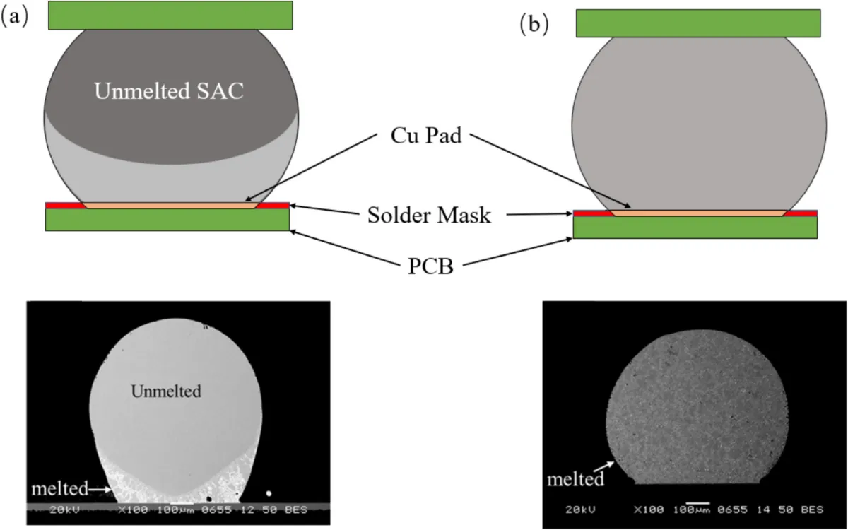
- Solder mask-defined (SMD): the land diameter is larger than the solder mask opening. After reflow, the molten solder ball contacts the solder mask edge.
- Non-solder mask-defined (NSMD, also called etch-defined or copper-defined): the solder mask opening is larger than the copper land. After reflow, the solder does not contact the solder mask.
SMD and NSMD behave differently under thermal and mechanical loads. NSMD lands typically deliver higher fatigue life because the solder wets to the copper edge, creating a more uniform fillet and reducing stress concentrations. SMD lands can reduce pad cratering in some non-critical nets, but they also introduce stress initiators at the mask edge and should be avoided on BGA package substrates and PCB lands where reliability is a priority.
1.1 SMD and NSMD Lands
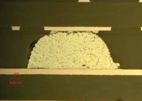
Figure 1 | Solder mask-defined (SMD) vs non-solder mask-defined (NSMD) BGA pad concepts
Possible cause: The BGA package substrate uses SMD lands while the PCB uses NSMD lands (or vice versa). A large difference in solderable area creates an asymmetric stress state in the solder joint. Cracks are likely to initiate on the SMD side at the solder mask edge. Oversized PCB lands reduce the likelihood of cracking but can introduce other assembly risks.
Potential corrective action: Keep the land definition consistent across the BGA substrate and the PCB. Avoid SMD lands on both sides of the interconnect unless needed for specific reasons such as mitigating pad cratering on non-critical nets.
1.2 Solder Mask Encroachment on Product Pads

Figure 2 | Solder mask encroachment onto the land on a production PCB
Possible cause: Excess solder mask encroaches onto the PCB land. This creates a local stress concentrator in the solder near the mask edge and promotes crack growth during temperature excursions.
Potential corrective action: Use NSMD lands for production boards unless SMD is explicitly needed to reduce pad cratering risk. Maintain adequate solder mask clearance and mask registration control.

Figure 3 | Crack initiates in the solder near the solder mask corner and propagates through the intermetallic compound (IMC) layer; nickel build-up is visible under the mask.
Possible cause: The crack originates at the solder mask's sharp corner due to stress focusing in the solder ball and then propagates through the IMC interface.
Potential corrective action: Prefer NSMD lands for BGA substrates and PCBs to avoid stress concentration at mask edges. Only use SMD to mitigate pad cratering on specific non-critical nets. For the same standoff height, NSMD lands can increase fatigue life by roughly 1.25–3×, with even greater benefit under severe loading.
SMD lands have three key drawbacks:
- Reduced effective land area and increased risk of top-side pad pull-away on the package substrate.
- Lower pad dimensional accuracy due to solder mask process tolerances.
- Reduced reliability because the mask edge acts as an early failure initiation site.
2. Excessive BGA Solder Ball Collapse
Molded (plastic) BGA solder balls typically collapse from an original height of about 750 μm to roughly 625 μm during package manufacturing, and then to around 500 μm after board-level reflow. If the package integrates a heat spreader or heat slug, the additional mass can compress the solder further—down to about 300 μm in extreme cases. Reduced standoff height lowers joint compliance and reliability, and the lateral spread of the solder can approach the pitch clearance. As a rule of thumb, initial reflow can reduce height by ~10% of ball diameter; with a heat spreader, the reduction can approach ~25%. Land geometry and solder mask clearance also influence collapse.
2.1 No Heat Spreader, 500 μm Standoff

Figure 4 | BGA solder ball geometry without heat spreader; ~500 μm standoff
Possible cause: The package weight is not sufficient to over-compress the solder balls. This is a target condition and a baseline for evaluating other balls on the same device or other BGAs.
Potential corrective action: If additional clearance is required, use spacers or mechanical support. Track and characterize solder collapse across builds.
2.2 With Heat Spreader, 375 μm Standoff
Possible cause: The package mass with a heat spreader increases solder collapse. Depending on the pitch, this deformation may still be acceptable if adjacent balls do not contact.
Potential corrective action: Use spacers or mechanical supports to prevent excessive collapse.
2.3 With Heat Spreader, 300 μm Standoff
Possible cause: The heat spreader weight has caused excessive collapse—this is a poor quality condition that must be corrected.
Potential corrective action: Use spacers or mechanical supports to limit collapse and restore standoff.
2.4 Solder Paste Volume — Critical for CBGA
Solder paste volume is helpful but not critical for molded BGAs because the solder balls themselves supply the solder. In contrast, for ceramic BGA (CBGA) with non-collapsing balls, sufficient solder paste is essential. For an 890 μm CBGA, a paste volume around 0.12 mm3 is recommended, with a minimum of 0.08 mm3. If paste volume is inadequate, joint reliability can be compromised. Paste must be supplied to wet to the high-temperature solder balls or columns, since the package termination solder volume does not contribute to joint formation.
2.5 Excessively Thick Paste Deposit
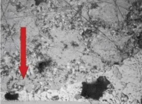
Figure 5 | Overly thick paste deposit in BGA region
Possible cause: Thick paste volume appropriate for non-collapsing ceramic balls was used with molded BGA balls.
Potential corrective action: Reduce stencil thickness; use a step-down stencil in the BGA area; reduce aperture size.
2.6 Voids by X-ray and Cross-Section
Transmission X-ray identifies voids (light areas) and their X–Y locations. It also reveals missing or irregular balls via differences in apparent diameter. However, determining the Z-axis (vertical) location of voids requires cross-sectional X-ray or microsection analysis.
2.7 Voids and Non-Uniform Balls

Figure 6 | X-ray example of voiding and non-uniform solder ball size
Possible causes:
- Excessive voiding within solder joints.
- Via-in-pad designs (per IPC-A-610, voids associated with via-in-pad are not necessarily considered defects).
- Overly fast temperature ramp in the reflow profile.
- Forward-compatibility mixing (Sn/Pb balls assembled with lead-free paste).
Potential corrective actions:
- Assess structural integrity by thermal cycling and/or microsectioning.
- Adopt a longer soak reflow profile.
- Eliminate the causal conditions listed above.
Voids arise from many causes. While representative voiding like this is common and not always a reliability risk, specific void morphologies can still pass extensive thermal cycling—for example, egg-shell voids have survived 1000 cycles (0–100 °C, no shock) in testing. Even when voiding does not reduce fatigue life in a given test, excessive voiding indicates problems with design, process, or materials. Verify product reliability accordingly.
2.8 Egg-Shell Voids

Figure 7 | Egg-shell void morphology in a BGA joint
0.65 mm microvia, 1000 cycles. The joint shows standoff collapse that led to intermittent contact opens.
Possible cause: Air or trapped gases during reflow. Gas can form and vent through microvias in the PCB.
Potential corrective action: Remove and replace the component.
3. Warpage (Bow and Twist) of the BGA Substrate
Molded BGAs are prone to warpage during normal reflow. Warpage can originate from the BGA substrate, the PCB, or both, stressing joints into opens or shorts. The reflow profile, package construction, solder paste volume, and cooling conditions all influence the risk. Corner shorts are an indicator of "frown" warpage (package corners downward), while corner opens suggest "smile" warpage (package corners lift). As packages and die get thinner, warpage effects increase.
To maintain a robust SMT process, ensure sufficient paste is deposited on all lands and monitor the process to avoid creating secondary defects like bridging and solder beads when compensating for warpage.
3.1 BGA Substrate Warpage
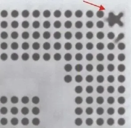
Figure 8 | Warpage (bow/twist) of a BGA substrate during reflow
Possible causes:
- Thermo-mechanical stress during reflow induces warpage.
- Similar conditions may be present at other corners—inspect all corners.
- "Frown" warpage (downward corners) can force corner balls into shorts; the inverse "smile" warpage lifts corner balls and causes opens.
Potential corrective actions:
- Increase corner ball size or use adhesive dots; in some cases, apply temporary tape/support during reflow.
- Return the package to the supplier for evaluation.
- Use shadow moiré or equivalent methods to check coplanarity at reflow temperature.
Corner opens indicate "smile" warpage, where the package lifts at the corners. While adding extra paste to the corner lands can reduce opens, it is not a root-cause fix. Only adjust stencil apertures as a last resort when the reflow process is already optimized and neither the package/substrate nor the PCB can be redesigned. Consider existing solder and component inventories before process changes. If additional paste is used to mitigate corner opens, monitor closely to avoid bridging, solder beads, and other side-effects.
3.2 Solder Joint Open Due to Substrate Warpage
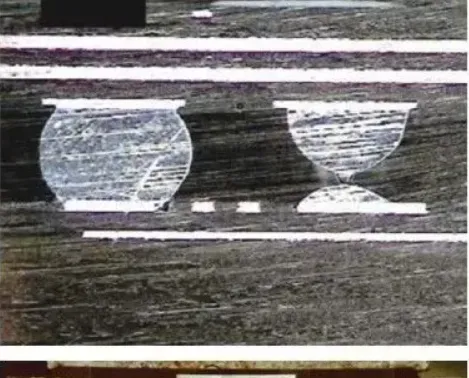
Figure 9 | Open corner joint associated with "smile" warpage
Possible causes:
- Insufficient paste release from the stencil or undersized solder balls.
- "Smile" warpage lifts corner solder balls.
Potential corrective actions:
- Inspect incoming packages for ball size and quality before assembly.
- Return suspect packages to the supplier; implement incoming inspection and/or supplier audits.
- Deposit additional paste on corner lands when redesign is not feasible.
4. Solder Joint Conditions and Defect Modes
The following examples relate solder joint appearance to assembly conditions and package/PCB interactions. Each includes the likely cause and recommended actions.
4.1 Target Joint Condition

Figure 10 | Uniform joint shape and texture, symmetric alignment; top and bottom of the ball have collapsed properly
Possible cause: Nominal condition with consistent shape, texture, and alignment—indicative of good wetting and collapse at both interfaces.
Potential corrective action: Standardize and control process parameters to maintain stability.
4.2 Over-Oxidized Solder Balls
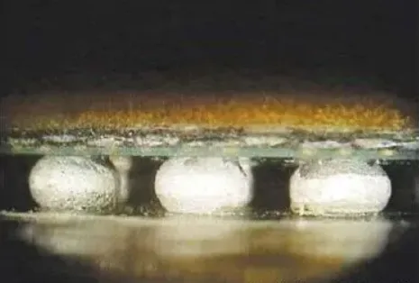
Figure 11 | Signs of oxidation on solder balls after repeated reflow exposure
Possible cause: Oxide formation on balls due to multiple reflow cycles (top-side and/or bottom-side) or prolonged high-temperature exposure.
Potential corrective action: Limit reflow to two passes when possible; choose flux chemistry appropriately; avoid cleaning between reflows that can exacerbate oxidation.
4.3 Dewetting Indicators

Figure 12 | Dewetting at the solder/land interface
Possible cause: Excess oxidation of the land, organic contamination, or poor plating quality. Black pad (electroless nickel immersion gold issues) can appear in both high-P and low-P systems; dewetting is driven by oxidation of the nickel barrier rather than just surface phosphorus content.
Potential corrective action: Design controlled experiments to isolate the dominant factor causing dewetting.
4.4 Mottled Surface

Figure 13 | Mottled solder surface appearance
Possible cause: Overheating during reflow or repeated exposure above liquidus, leading to surface texturing on the solder.
Potential corrective action: Re-evaluate the reflow profile to achieve target solder characteristics without overexposure.
4.5 Sn/Pb Solder Balls — Evaluation
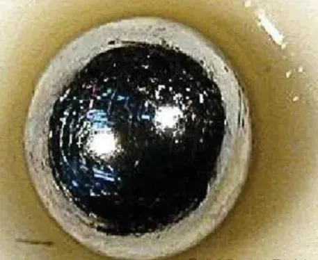
Figure 14 | Expected ball geometry with Sn/Pb solder after reflow
Possible cause: Representative good joint if the reflow process forms proper ball shape and wetting.
Potential corrective action: Maintain standardized process controls.
4.6 SAC Alloy Appearance
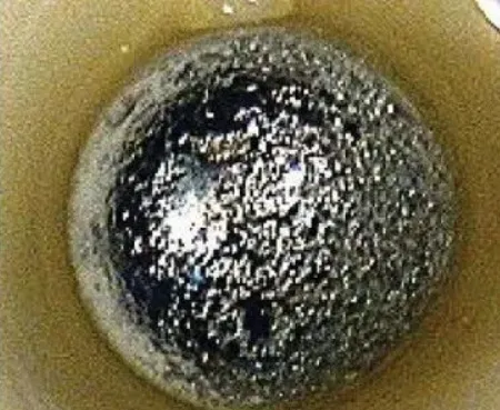
Figure 15 | Slight speckling typical of SAC (Sn-Ag-Cu) solder appearance
Possible cause: Normal SAC surface texture.
Potential corrective action: Characterize and control paste and ball alloy attributes through experiments.
4.7 Cold Solder Joint
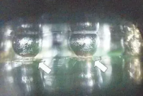
Figure 16 | Cold joint: incomplete wetting at the contact interface
Possible cause: Incomplete wetting due to poor paste printing or contamination preventing wetting at the land.
Potential corrective action: Inspect stencil condition and printing process; ensure adequate paste deposition and good land cleanliness.
4.8 Incomplete Joint Due to Land Contamination

Figure 19 | Incomplete joint formation caused by land oxidation/contamination
Possible cause: Organic contamination or oxidized PCB lands prevent uniform and complete joint formation. Lands were not sufficiently clean prior to paste application.
Potential corrective action: Include cleanliness testing in the process. Implement proper PCB storage and handling to prevent contamination and oxidation.
4.9 Contamination from Deformed Solder Balls
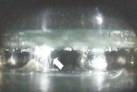
Figure 18 | Deformed balls from package movement or incorrect land geometry
Possible cause: Package or board movement during reflow (warpage) and/or improper land geometry causes ball deformation.
Potential corrective action: Avoid overheating that exacerbates substrate warpage and material variation; verify land geometry.
4.10 Columnar (Deformed) Solder Balls

Figure 19 | Columnar joints: package corners lift during reflow (dynamic warpage)
Possible cause: Transient package warpage during reflow (dynamic warpage) lifts corners away from the PCB. As the alloy cools and solidifies, joints freeze into columnar shapes. On cooling, the package may recover if not constrained by solidified solder.
Potential corrective action: The primary driver is CTE mismatch between package and PCB materials. While complete elimination may be outside SMT control, minimizing overheating reduces warpage magnitude.
4.11 Insufficient Solder and Flux

Figure 20 | Suspended ball: insufficient solder and flux to form a joint
Possible cause: Paste under-deposition from stencil print leads to insufficient solder and flux. The interface did not reach full liquidus on both sides.
Potential corrective action: Inspect stencil, confirm paste deposition volume, and verify flux activity in the paste.
4.12 Reduced Terminal Contact Area

Figure 21 | Columnar joints in the center with adjacent balls retaining spherical shape
Possible cause: Local package lift (warpage) in the illustrated region. The center joints stretch into columns while adjacent joints remain more spherical.
Potential corrective action: Control package movement during solidification and avoid overheating in reflow.
4.13 Solder Bridging

Figure 22 | Solder bridge between adjacent contacts
Possible cause: Paste residue transfer during printing or poor stencil-to-board gasketing allows excess paste to remain between contacts.
Potential corrective action: Review stencil apertures and reduce paste volume where necessary.
4.14 Incomplete Reflow

Figure 23 | Incomplete reflow: solder ball and paste did not fully liquefy and coalesce
Possible cause: The solder ball on the package and the paste on the PCB did not both reach full liquidus during reflow.
Potential corrective action: Verify the reflow profile against the paste specification and ensure adequate time above liquidus.
4.15 Open Joint (Missing Paste)

Figure 24 | Open joint caused by insufficient paste on the PCB land
Possible cause: Paste was not deposited on the land, preventing proper joint formation. During reflow, the deposited paste must melt and combine with the ball to form a joint.
Potential corrective action: Check for clogged stencil apertures; ensure correct aperture design for every SMT land.
4.16 Non-Wetting Open

Figure 25 | Non-wetting open (NWO) on a BGA joint
Possible cause: Clogged stencil apertures, BGA warpage, and paste chemistry interactions.
Potential corrective actions:
- Use automated inspection to monitor paste volume.
- Select paste chemistry/alloy tailored to mitigate NWO risk.
- Overprint paste in risk areas (package corners); minimize board warpage (e.g., with carriers/pallets).
4.17 Head-in-Pillow (HoP)
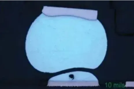
Figure 26 | Head-in-pillow (HoP) defect
Possible cause: Interaction of BGA and PCB warpage with insufficient time above liquidus (TAL) during reflow.
Potential corrective actions:
- Overprint paste in risk areas (BGA corners).
- Reduce component temperature deltas; increase peak temperature and TAL.
- Reflow in a nitrogen (N2) atmosphere; select paste chemistry/alloy to mitigate HoP.
- Reduce board warpage (e.g., use support pallets).
Reference: IPC-7095, Design and Assembly Process Implementation for Ball Grid Arrays