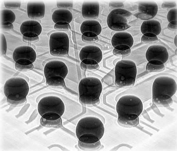
As electronics become thinner and smaller, component terminations and PCB pads continue to shrink. This trend places increasing demands on solder paste printing. Paste printing quality is the core of SMT process control and is responsible for an estimated 60–70% of SMT defects. In practice, overall product yield is often determined by a handful of micro joints. Ensuring robust printing and soldering quality on these micro pads must therefore be a central focus.
Observed Pads, PCB Features, and Typical Defects
In the micro-feature domain, some pads consistently suffer missing print or insufficient solder after reflow, even when larger neighboring pads print well. Visual inspection commonly reveals these recurring characteristics:
- Non-solder mask defined (NSMD) pads with apertures larger than the copper pad area.
- Pads near outer-layer traces where the solder mask over copper stands higher than mask over bare substrate.
- Annular "trenches" around pads: the area between the pad edge and surrounding solder mask sits lower, effectively forming a ring-shaped recess.
On affected pads, paste volume is often significantly lower than expected or absent entirely, while pads of similar size connected to routing tracks tend to print more consistently.
Why Micro Pads Miss or Lose Paste: Mechanism and Analysis
How Solder Paste Transfers During Printing
During printing, the squeegee forces paste into the stencil apertures. Good transfer requires the paste at the bottom of each aperture to contact and adhere to the PCB surface. As the stencil separates (release), the paste that is well-adhered to the PCB overcomes the friction on the aperture walls and transfers onto the board. If paste at the aperture bottom does not contact the PCB (or the contact area is too small), adhesion to the stencil walls dominates, and paste remains in the aperture. The result is missing print or insufficient paste on the pad.
The Role of Stencil-to-Board Gap Caused by Solder Mask Topography
Real PCBs do not present a perfectly flat surface to the stencil. Solder mask deposited over copper features (e.g., traces) is typically higher than mask applied directly over the substrate. When an NSMD pad is near a trace, the elevated solder mask on the trace can locally lift the stencil. This creates a stand-off between the stencil bottom and the PCB where the aperture extends beyond the copper pad into the surrounding substrate area.
Cross-sectional observation of problematic locations often shows an annular recess between the pad edge and solder mask—an approximately 35 μm-deep ring-shaped trench. Where the stencil aperture lies above this trench or bare substrate, the stencil-to-board gap is largest. Paste in those regions fails to contact the PCB during the print stroke and, on release, tends to stay in the aperture instead of transferring to the pad.
Why Pads Connected to Traces Print Better
Pads that are directly connected to outer-layer routing typically have more of the aperture area over copper rather than over substrate. That increases the likelihood of paste contacting metal at the aperture bottom even with some local stand-off. The paste can wet and adhere to copper, improving transfer during stencil release. Conversely, isolated pads without nearby copper under the aperture suffer larger effective gaps in the overhang region, reducing contact and transfer efficiency.
Zero-Gap Assumptions Behind Aperture Sizing
Aperture sizing guidelines such as the IPC-7525 area/coverage criteria assume "zero-gap" printing, meaning the stencil forms a tight gasket on the PCB surface. When a local stand-off exists, those criteria no longer guarantee reliable transfer. If the aperture is larger than the copper pad, the portion of the aperture over bare substrate is at the highest risk of non-contact and poor release. This explains why, despite following area-ratio guidelines, micro pads near topographical variation can still miss print or receive insufficient paste.
Evidence From Bare-Board Printing
To separate PCB topography effects from paste and stencil factors, bare-copper printing tests were performed. Five different brands of Type 4 solder paste all printed consistently through a laser-cut, electropolished stencil with 0.1 thickness and a circular aperture of 0.28 diameter. On the flat, mask-free copper surface, transfer was stable and repeatable, indicating that the paste rheology and aperture quality were adequate.
Combined with cross-sectional observations, these results support the following conclusions:
- Solder mask topography creates a real, local stencil stand-off on assembled PCBs. This stand-off is absent on bare copper, where printing succeeds under the same paste and aperture conditions.
- The largest gap typically appears where the aperture extends beyond the pad onto the substrate in the annular trench zone. Paste in this region does not contact the board and fails to transfer.
Key Takeaways
The root cause of recurring missing print and insufficient solder on micro pads is the printing gap induced by solder mask topography and nearby copper features, especially around NSMD pads with apertures larger than the pad. This issue is easy to overlook because aperture sizing rules are often applied assuming a flat, zero-gap interface. Eliminating local printing gaps—particularly those caused by routing and solder mask height differences—is critical to stabilizing paste deposits on micro pads.
Corrective Actions and Design-for-Print Recommendations
1) Adjust Pad Geometry for Isolated Micro Pads
Identify all pads not connected to outer-layer routing. Increase their pad diameter from 0.27 to 0.31 (same aperture retained) so that the previous overhang region above the annular trench now lies over copper. This reduces the stencil-to-board gap under the aperture. After small-lot validation, mass production using the original stencil achieved robust deposits on pads that previously struggled to take paste. No solder bridging was observed during volume builds in this case.
2) Control Solder Mask Thickness
Reduce solder mask thickness to lessen the relative height over copper features near pads. Keeping the mask thickness below 25 μm helps minimize stencil lift in critical regions, improving gasket seal and paste contact in the aperture overhang area.
3) Use Stencil Technologies That Minimize Stand-Off
Adopt a stencil designed to maximize sealing to the PCB and minimize local stand-off at micro features. The stencil variant shown below (often referred to as a PH stencil) is intended to reduce the printing gap and improve paste transfer on micro pads near solder mask topography.
Industry Standards and Practices From High-Yield Manufacturers
Solder Mask Thickness Criteria
Many PCB manufacturers qualify solder mask thickness per IPC-SM-840C. Under this standard, Class 1 products have no specified limit, Class 2 products require a minimum thickness of 10 μm, and Class 3 products require a minimum thickness of 18 μm. For micro-feature printability, tighter control below these minima at critical regions can improve outcomes by reducing stencil stand-off. Where practicable, specifying a maximum local thickness in fine-pitch areas helps.
HDI and Pad Strategy for Sub-0.4 Pitch BGA
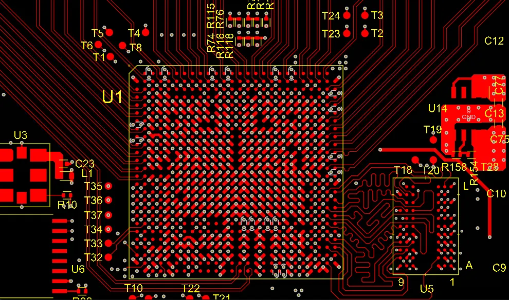
For BGAs below 0.4 pitch, mobile-industry designs commonly adopt HDI practices such as via-in-pad to route signals without surface traces near pads. Using NSMD pads combined with blind microvias filled, planarized, and plated within the pad prevents raised solder mask over nearby traces from lifting the stencil and creating a gap.
End-to-End DFM Measures for Fine Pitch
For fine-pitch components such as 0.4 pitch BGAs, the following integrated measures from high-yield practitioners address PCB-induced printing gaps at the source:
- Omit white legend (silkscreen) in critical micro-feature areas; expose copper instead.
- Control solder mask thickness to below 25 μm in fine-pitch regions to reduce stencil lift.
- Use NSMD pads and route with via-in-pad (microvia fill, planarization, and plating) to eliminate surface traces adjacent to pads.
- Pair the above with a stencil strategy that improves sealing and release on micro pads.
Practical Notes for Process and Design Teams
- Do not assume that meeting aperture area-ratio guidance guarantees print success at micro scale. Those criteria presume zero-gap printing. Verify local topography and seal quality at critical pads.
- When an aperture is larger than the pad, the overhang region is the highest-risk area for non-contact. Reducing or eliminating overhang above substrate by modestly enlarging the pad can dramatically improve transfer without necessarily increasing bridge risk, subject to validation.
- If certain pads consistently show missing or low paste while others print well, inspect for nearby copper features and solder mask height differences lifting the stencil locally. Cross-sectioning or 3D optical profiling near the defect is often revealing.
- Validate with bare-copper printing when in doubt. If bare-board results are stable across pastes and stencil conditions, suspect PCB topography at the assembled board level.
Micro-pad print stability is ultimately a system problem spanning PCB fabrication, pad design, solder mask control, and stencil technology. Addressing the local stencil-to-board gap—especially where solder mask over copper is higher than over substrate—eliminates the primary mechanism behind missing print and insufficient solder on micro pads in modern, miniaturized electronics.