Solder opens on SMT connectors are a familiar but often stubborn class of defects. Even on mature products, a sudden spike in connector-related opens can be difficult to troubleshoot because multiple factors—stencil design, coplanarity, reflow profile, and component construction—interact during reflow. This case study documents a 100% solder-open failure on a CF Card SMT connector, the diagnostic steps taken across process and materials, and the corrective actions implemented with the component supplier. Although the final fix appears straightforward in hindsight, arriving at a robust solution required systematic analysis.
Defect Description
The assembly had been in volume production for a long time before the failure emerged. The observed defect was:
- Yield impact: 100% solder opens on the CF Card connector during SMT.
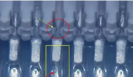
- Failure pattern: All opens were concentrated at the middle pins; the outer pins on both ends did not show open-solder defects.
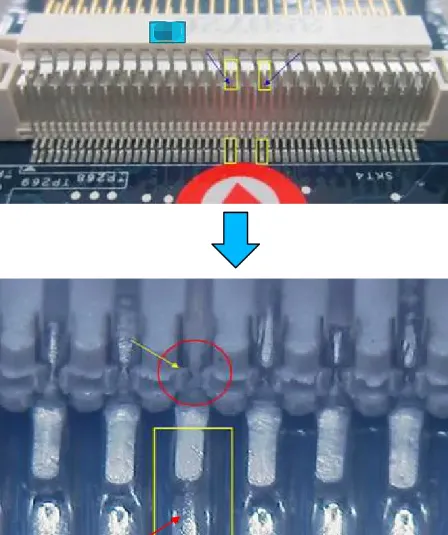
Figure 1 | Solder opens concentrated at the middle pins of the CF Card connector; end pins are unaffected.
Root Cause Analysis
Because the product had a stable history, the first hypothesis was a lapse in manufacturing control. The production process was therefore reviewed end-to-end, followed by targeted experiments to rule out process variables before switching to materials and component structure.
Process verification
Solder paste printing, component placement, and reflow parameters were comprehensively checked. All recorded parameters and in-process inspection data met control limits. Multiple DOE cycles were then conducted to optimize process windows and stencil apertures, but the opens on middle pins persisted. Efforts to increase local solder volume even produced new bridging defects in some trials. These results pointed away from a simple process window issue and toward a component-related mechanism.
Component Coplanarity Assessment
Given the location-specific nature of the failures, coplanarity was an obvious suspect. Coplanarity refers to how well all leads lie on the same plane. If some pins sit higher than others, the effective gap to the pad increases. During reflow, solder paste collapses and wets the lead and pad; if the gap is too large, the solder may not bridge the gap to form a reliable joint, resulting in an open.
Pre-reflow coplanarity check
To quickly screen the incoming components, a practical method was used in lieu of dedicated metrology equipment: several connectors were placed onto bare PCBs (no solder paste) and the lead planarity was visually checked. No obvious "high-up" leads were observed on the five samples, suggesting that incoming coplanarity before any thermal exposure was acceptable.

Figure 2 | Quick screening method: place the connector on a bare PCB to observe lead flatness before reflow.
Post-reflow coplanarity measurement
Because the observed opens occurred after reflow, the next step was to test whether the component deformed thermally. Connectors were reflowed on bare boards with the normal production profile (no solder paste). After cooling, an IQC coordinate-measuring system was used to measure the flatness difference between middle and end pins. The middle pins showed an average "high-up" of approximately 0.05 mm compared to the ends.
This confirmed that the connector's middle leads warped upward through the thermal cycle. Moreover, deformation measured at room temperature after cooling tends to understate the peak deformation that occurs near the reflow apex, because metal and polymer materials relax differently during cooling. In other words, the gap present at liquidus is likely larger than what is measured post-cooldown, which is precisely when solder wetting must bridge the lead-to-pad gap. This thermal deformation explains why the opens were isolated to the connector's middle pins.
Mechanism: Why the Middle Pins Lift
Long SMT connectors undergo nonuniform expansion during heating. The plastic housing and metallic terminals have different coefficients of thermal expansion (CTE) and moduli that change with temperature. As the assembly passes through the reflow peak, the plastic approaches or exceeds its glass transition region, its stiffness drops, and internal stress redistributes. The terminals, constrained by the housing and any local resin staking, can release stored stress by lifting away from the pad plane. Geometrically, the middle of a long body is less laterally constrained than the ends; the ends also benefit from additional mechanical support at the connector frame, which is why deformation concentrates in the center.
The practical effect is an excessive lead-to-pad gap at the moment solder needs to form a metallurgical bond. Increasing solder paste volume can sometimes compensate by providing more collapse and wetting, but on fine-pitch arrays this also raises the risk of solder bridging. The DOE trials in this case confirmed the trade-off: more paste reduced some opens but introduced bridges, failing to deliver a robust process window.
Analysis of Out-of-Spec Components
To dive deeper, suspect components with coplanarity out of spec were examined. Two structural observations stood out:
- The terminal did not contact the plastic wall; a gap of about 0.2 mm was observed. A dimension nominally 0.8 mm was found at 0.95 mm. This implies the terminal's thermal stake depth was shallow, leaving a clearance between the molten resin and the terminal. During reflow, as stress relaxes, the terminal tends to settle against the softened resin rather than the plastic wall, effectively "lifting" and degrading coplanarity.
- The resin layer covering the terminal lacked sufficient mechanical strength under reflow temperatures. When the terminal tries to expand or rotate due to stress relief, it exerts an outward force on the resin. At elevated temperature, resin modulus drops, and the coverage cannot restrain the terminal, allowing it to lift further and create a large gap over the pad plane.
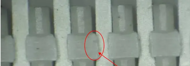
Figure 3 | Terminal lift mechanism: stress relief during reflow overcomes insufficient resin restraint, producing coplanarity loss at the middle pins.
Corrective Actions with the Component Supplier
Based on the above mechanism, the connector needed stronger mechanical restraint of the terminals in the region most prone to thermal deformation. The agreed corrective actions were to increase both the depth and the area of the thermal staking so that more resin encapsulates the terminal and maintains its position through the reflow peak.
Design changes
- Increase thermal stake depth to raise the volume of resin covering the terminal, thereby increasing structural strength around the lead.
- Increase the hot-melt head width from 0.5 mm to 0.8 mm to enlarge the resin coverage area and improve restraint during thermal cycling.
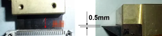
Figure 4 | Connector improvements: deeper thermal staking and wider staking head increase resin volume and coverage to restrain terminals.
Results and Verification
The PCB supplier produced 100 pieces incorporating the design change for straight-through verification on the SMT line using the normal reflow profile and production setup. The lot achieved 100% yield with zero solder opens or bridges. Subsequent mass production with the modified connectors maintained a stable, defect-free process. The issue was fully resolved.
Practical Lessons and Recommendations
This case highlights several practical takeaways for diagnosing and preventing connector-related solder opens:
- Separate process and component factors early. If a design has previously been stable, a rapid process check followed by focused DOEs can determine whether stencil and profile adjustments have the leverage to solve the problem without creating new defects such as bridging.
- Measure coplanarity after reflow exposure, not just at incoming inspection. Thermal deformation is often the hidden driver of mid-row opens on long connectors. Reflowing sample parts on bare boards and measuring planarity after cooldown is a simple, revealing test. Keep in mind that actual lift at the reflow peak can exceed the post-cooldown measurement.
- Understand the structural restraint of terminals inside the connector. Coplanarity depends not only on lead geometry but also on how the terminal is staked and encapsulated by resin, especially near the center of long bodies where thermal and mechanical constraints differ from the ends.
- Use paste volume judiciously. Increasing aperture size can sometimes mask marginal coplanarity, but on fine-pitch connectors it easily trades opens for bridges. When opens concentrate in the middle of long rows, a structural fix at the component is usually more robust than relying on paste volume.
- Collaborate with suppliers on targeted design changes. Increasing thermal stake depth and coverage area directly addresses lift by raising resin stiffness and contact area around the terminal. Request dimensional verification and, where possible, cross-sections or mechanical retention tests to confirm the intended restraint has been achieved.
- Maintain a feedback loop. Once the change is validated on a pilot lot, track performance in mass production to confirm that yield remains stable across date codes and manufacturing conditions.
Connector solder opens rarely have a single universal cause, but the pattern of failures—middle pins only, long body, fine pitch—often points to thermally induced coplanarity loss. Verifying deformation through a reflow cycle and strengthening the terminal restraint inside the connector provide a reliable path to permanent correction.