Quad Flat No-Lead (QFN) packages are widely used for their low profile, excellent thermal performance, and small footprint. However, because the terminals are primarily located on the package underside, ensuring robust side-wetting on the leadframe flanks during SMT assembly can be challenging—especially when oxidation or singulation artifacts degrade solderability. This article analyzes common QFN package structures, side-wetting mechanisms and process controls, and key factors that drive solder joint reliability at the board level.
Typical QFN Package Structure
Molded QFN devices are typically built on a copper leadframe with conductive die attach, a bare die, bond wires, and an epoxy molding compound. Electrical terminations are on the bottom of the package, and plating finishes are commonly Sn or NiPdAu.
QFN leadframes are singulated either by punching (stamping) or by sawing (cutting). Saw singulation leaves the side of the leads as bare copper. During subsequent screening and storage, the exposed copper easily oxidizes, reducing solderability and causing poor side-wetting in reflow. Stamping may leave smears or residual tin on the upper portion of the flank. Because this residual tin is not an electroplated metallurgical coating, it is not reliably bonded to the copper leadframe and can also oxidize during handling and storage. Process flows for saw and punch singulation.
By terminal geometry, QFN variants may also be categorized as having recessed terminals vs non-recessed terminals. Terminal geometry influences assembly process windows and the ability to form a visible side fillet.
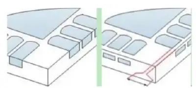
Figure | Recessed vs non-recessed terminal geometry
The following sections focus on side-wetting behavior on the QFN flank and its impact on solder joint reliability, with the aim of providing practical guidance for device selection and high-reliability assembly.
Side-Wetting Behavior of QFN Flanks
Because the QFN flank is exposed copper after singulation, it readily oxidizes during singulation, screening, and storage. This reduces solderability and impairs the formation of a robust side fillet during reflow. Although mainstream electronics assembly standards (such as IPC-A-610 and IPC-7093) do not mandate a side fillet height, high-reliability applications often specify stringent side-wetting heights—75% is common, and some programs require 100%—to stabilize both electrical and mechanical performance. 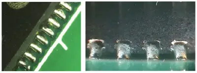
Figure | Example of good side-wetting on QFN flanks
Industry studies point to several effective approaches for achieving consistent side fillets on QFN flanks:
1) Solder paste printing quality
Using a Six Sigma, two-level full-factorial design of experiments, researchers found solder paste printing quality to be the most significant factor affecting side-wetting height, followed by whether the flank was pre-tinned prior to assembly.
2) Side-wettable flank QFN packages
Compared with conventional QFN, side-wettable flank QFN devices incorporate a specially designed flank geometry and tin finish on the sidewall. This mitigates burrs and copper exposure inherent to saw singulation, creates a favorable wetting angle, and enables reliable AOI inspection of the side fillet after reflow. These features strengthen solder joint quality and suit high-reliability requirements.
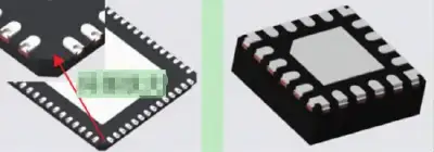
Figure | Example of a side-wettable flank QFN
3) Chemical pre-tinning after singulation
Electroless tin plating on the exposed copper flank after singulation has been demonstrated to form a solderable tin layer on the sidewall. Solderability tests confirm that the treated flank can form a good wetting angle in reflow. 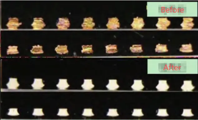
Figure | Exposed flank before vs after electroless tin plating
4) Hot-dip tinning pre-coat
Hot-dip tinning has been used to pre-tin the exposed copper flank; however, results depend strongly on the surface condition of the copper. Severely oxidized areas may not accept solder, compromising subsequent assembly. In addition, the porous morphology of such deposits increases the risk of tin whiskers during storage. Overall, hot-dip tinning has significant limitations when flank oxidation is severe.
5) Hand pre-tinning by soldering iron
Hand pre-tinning with a soldering iron has been used to address flank pre-tin on oxidized QFN terminals. However, this approach can induce delamination failures at the leadframe interface. Mitigations include reducing soldering temperature and roughening the leadframe surface to improve adhesion.
6) Flux cleaning and reflow
Systematic comparisons of soldering iron pre-tinning, acid pickling, and flux-assisted reflow cleaning on oxidized QFN flanks indicate that flux reflow cleaning is effective for production. After flux reflow cleaning, the side-wetting rate reached 100%, and 96% of joints achieved side-wetting heights greater than 75%, significantly improving pass rate for oxidized flanks.
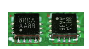
Figure | Side-wetting and yield after flux reflow cleaning
7) Nano solder paste
The activity and chemistry of the flux system strongly influence solderability. In conventional solder paste, flux particles are larger than the solder powder, and solder powder agglomeration can occur, degrading printing and reflow results. When flux solids are processed to nanoscale—smaller than the solder particles—liquid bridging distributes active species more uniformly across solder particle surfaces, enhancing deoxidation at the interface. Incorporating nano-scale additives (e.g., nano Ni, nano Cu, or other metals) can further tune paste behavior. Nano-treated flux reduces agglomeration, improves stencil release, and significantly increases oxide removal capacity, improving side-wetting on QFN flanks.
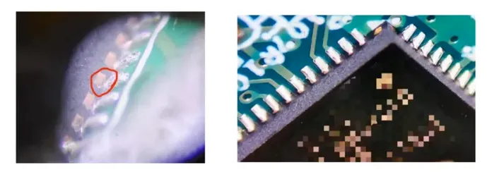
Figure | Side-wetting comparison: standard vs nano solder paste
8) PCB land pattern optimization
To mitigate insufficient side fillet height and similar defects, both PCB land design and stencil design should be optimized. As a rule of thumb, land pads should be slightly larger than the QFN terminations: pad widths on the order of 0.25–0.50 mm and lengths of 0.60–0.96 mm are commonly used. To ensure toe fill, extend the land outward by 0.1–0.2 mm and inward by more than 0.05 mm. Maintain at least 0.2 mm clearance between adjacent signal lands and between signal lands and the central thermal pad to avoid bridging.
9) Stepped flank structure
Stepped (notched) flank designs on wettable-flank QFN (WFQFN) packages improve solder capillary action and side-wetting. Simulated solder flow experiments show that when the step depth is ≥0.05 mm and the step width is ≥0.02 mm, wetting and side-fillet height improve markedly, providing better soldering outcomes.
Solder Joint Reliability of QFN Assemblies
1) Effect of device size
Under deep-space simulated conditions, NASA analyzed the impact of QFN package size on solder joint life under thermal shock using Weibull statistics. Results show that larger QFNs exhibit significantly shorter solder joint life than smaller QFNs under identical test conditions. For deep-space applications, the large-format QFN package should be avoided.
2) Effect of molding compound CTE and flank wetting
The coefficient of thermal expansion (CTE) of the package body strongly influences solder joint life. Studies examining molding compound CTE (7×10⁻⁶/°C vs 12×10-6/°C), solder type (SnPb vs SnAgCu), and flank wetting (wettable vs non-wettable) indicate the package body material has the most pronounced effect. In reported results, the device with a 12×10-6/°C body CTE had three times the solder joint life of the 7×10⁻⁶/°C variant. By comparison, the solder alloy and flank wetting condition affected life by less than about 20%. For high-reliability designs, pay close attention to the molding compound CTE.
3) Effect of PCB mounting and layout
As a leadless package, QFN solder joints are more sensitive to board-level mechanical stress. Mounting method and local rigidity can significantly affect reliability, particularly in systems where the PCB is fastened into a housing or cavity. Tests that bolted QFN-populated PCBs to a 4 mm aluminum plate showed that, under -40 to 125 °C thermal cycling, unfastened boards had higher solder joint life. Joints located closer to mounting screws failed earlier. In practice, the thermal expansion and stiffness of the enclosure, coupled through fasteners, drive local strain at QFN joints. Place QFN components away from mounting screws and avoid structures that concentrate stress in the device area.
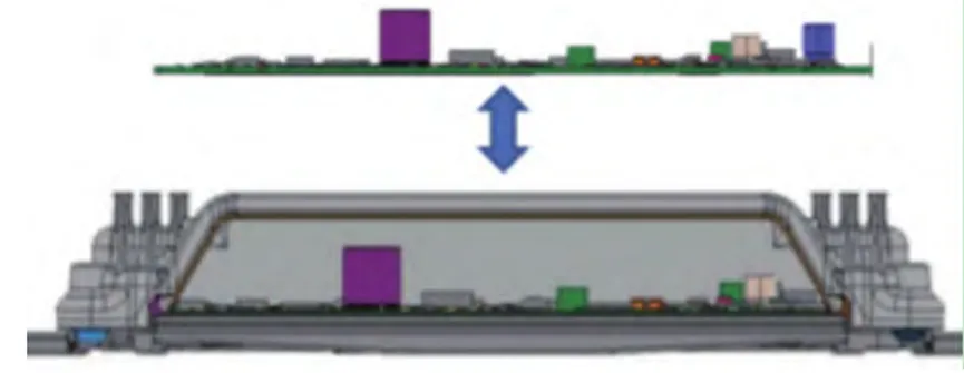
Figure | PCB cavity mounting illustration
4) Effect of conformal coating
Conformal coating is frequently applied in high-reliability products. Coating thickness and material can markedly impact QFN solder joint life under thermal cycling. Some studies report that under -55 to 125 °C cycling, uncoated QFN joints survived approximately 2,000–2,500 cycles, whereas coated joints survived roughly 300–700 cycles, though device sizes and materials were not fully detailed. Comparative tests using polyurethane vs acrylic coatings found polyurethane-coated samples exhibited significantly higher solder joint life than acrylic-coated samples, and coating effects interacted with device materials and size. Cracks typically formed within the bulk solder.
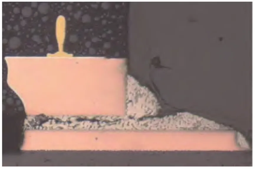
Figure | Crack within bulk solder after coated thermal cycling
Further work on acrylic coatings shows crack initiation near the joint root, with longer cracks and more cracked joints compared to uncoated samples under the same thermal cycling profile. Analyses attribute the acceleration to coating-induced constraint at the package bottom, increasing joint deformation and driving crack initiation and propagation during temperature swings. For assemblies populated with larger QFNs, rigorously validate coating materials and thicknesses to avoid unintended reliability degradation.
5) Design-driven factors at the component and board level
Board-level studies indicate that a target post-reflow QFN solder joint standoff (height) of about 2–3 mil helps improve reliability, with a desirable toe fillet on the flank side. From a component selection standpoint, favor smaller package sizes, smaller die area and thickness, and a larger pin pitch to reduce stress and warpage coupling. At the board level, follow IPC-7093 recommendations, reduce PCB thickness where feasible to limit constraint, and minimize QFN temperature excursions during use. Also, avoid PCB warpage and local stiffness transitions that add mechanical stress to the joints. Simulation comparisons of key factors are summarized.