Head-in-Pillow (HIP) is a typical failure mode in BGA (ball grid array) and CSP (chip-scale package) reflow soldering. It presents as incomplete fusion between the solder ball and solder paste, forming a partial, "head resting on a pillow" interface that behaves like a cold joint. HIP is highly latent and may pass functional testing, yet it is prone to intermittent opens and mechanical-stress-induced failure over time, undermining long-term product reliability. The following provides a systematic analysis and practical mitigation strategies.
How HIP Forms: Mechanisms and Primary Causes
Thermal Deformation and Warpage
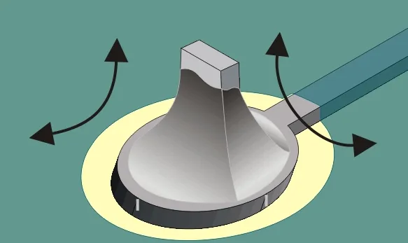
BGA or PCB warpage during reflow: When the package substrate and PCB have mismatched coefficients of thermal expansion (CTE), or when the temperature ramps too quickly, localized bow/warp can occur during reflow. This transient deformation physically separates the molten solder ball from the printed solder paste. As the assembly cools, the ball and paste re-contact, but oxide films that formed during separation inhibit metallurgical bonding, leaving a HIP interface.
High-risk regions: HIP is overwhelmingly concentrated in the outer 1–3 rows of BGA balls, where warpage is typically greatest.
Solder Ball and Pad Surface Conditions
Oxidation or contamination: Residues from package test probes, storage humidity excursions beyond the MSL rating, and incomplete cleaning of water-soluble fluxes can all promote oxidation on solder balls (e.g., SnO/SnO2), increasing the risk of non-wet or partial-wet interfaces during reflow.
Secondary oxidation at temperature: At elevated temperatures, flux activity can be depleted. Once the flux no longer protects the molten solder, oxidation accelerates on the solder surface, further degrading wetting and fusion.
Process Parameter Imbalances
Solder paste printing defects: Undersized stencil apertures, print misregistration, and via-in-pad structures that wick solder away can all cause insufficient or uneven solder paste deposit volume under the BGA, increasing HIP susceptibility.
Improper reflow profile: Excessive preheat time (> 100 s) or excessive preheat temperature (> 200 °C) can drive off flux volatiles and reduce flux activity before peak. Peak temperatures that are too high (> 240 °C) exacerbate oxidation and mechanical deformation (warpage) in both the package and PCB.
Material Compatibility Issues
Low-activity solder pastes: Pastes with weaker high-temperature oxidation resistance (e.g., certain Bi/In alloy formulations) may provide insufficient wetting and oxide reduction under BGA balls, elevating HIP risk.
Low-Tg PCB laminates: Boards with lower glass transition temperatures soften more readily at reflow temperatures, making them more prone to deformation and coplanarity loss under heavy BGA components.
Detection and Diagnosis of HIP
| Method | Principle and Advantages | Limitations |
|---|---|---|
| 3D X-ray CT | Tomographic reconstruction of the joint's 3D structure reveals vertical non-fusion regions characteristic of HIP. | High equipment cost and slower throughput. |
| Red-dye test | Penetrant dye wicks into unbonded gaps; after separation, dyed regions indicate non-fusion. Destructive but high accuracy. | Destructive, with more complex processing (vacuum infiltration and thermal cure required). |
| Cross-section analysis | Sectioning through the joint and observing under an electron microscope reveals unbonded interfaces and void morphology. | Destructive; suitable only for sampling analysis. |
| 2D X-ray | Tilted imaging (e.g., ~45°) can reveal "gourd-shaped" trailing indicative of HIP-related mass distribution. | Insensitive to purely vertical separation; prone to missed detection. |
Note: Functional testing (ICT/FVT) and burn-in can screen some intermittent HIP-related failures, but overall coverage is limited.
Solutions and Prevention Strategies
Optimize Stencil Design and Solder Volume
Increase paste volume selectively at outer rows: For the outer 1–3 rows of BGA pads, consider changing stencil apertures from circular to square inscribed apertures to boost paste volume (for example, 0.26 mm round aperture to 0.25 mm square yields an approximate 13.6–24.97% increase in deposit volume). Maintain circular apertures in the central rows to avoid excessive solder and bridging.
Improve stencil area ratio (AR): Ensure AR > 0.66 to maintain reliable paste release and avoid insufficient solder deposits under fine-pitch BGAs.
Upgrade Solder Paste and Flux Activity
Use solder pastes with higher oxidation resistance: For instance, SAC305 (Sn-Ag-Cu) may offer stronger resistance to high-temperature oxidation than some low-silver or low-activity formulations, improving wetting under BGA balls. In one case, changing the paste reduced HIP defect rates from 3% to 0%.
Enhance the reflow atmosphere and local activation: Nitrogen reflow (O2 < 500 ppm) inhibits oxidation of molten solder and exposed copper land surfaces. Where applicable, targeted flux deposition can directly activate the ball surface and improve fusion.
Control the Reflow Profile Precisely
Shorten the preheat dwell: Maintain the 150–200 °C soak range within approximately 60–80 seconds (instead of > 100 seconds) to preserve flux activity into the peak zone.
Lower the peak temperature: Set peak to approximately 235–240 °C to reduce high-temperature oxidation and mitigate package/PCB warpage while still achieving full solder melt and wetting.
Warpage Suppression and Materials Control
Use carriers/fixtures through the oven: For thin (≤ 1.0 mm) or large PCBs, a dedicated carrier can provide mechanical support during reflow (especially on the second pass), limiting board sag and warpage under BGAs.
Select higher-Tg board materials and manage moisture: Choose laminates with Tg > 170 °C to improve high-temperature rigidity. Bake incoming BGAs (e.g., 105 °C for 4–8 hours) to remove absorbed moisture and reduce warpage or popcorn risks during reflow.
Collaborate with component suppliers: Specify package warpage control at reflow temperatures (e.g., high-temperature deformation < 80 μm). Require non-water-soluble flux usage in ball-attach processes to minimize ionic residues and oxidation risks at the solder ball interface.
Practical Implementation Advice
- Prioritize low-cost, high-impact levers: Start with stencil optimization and solder paste selection, which typically deliver fast improvements at modest cost. Tune the reflow profile next. Consider carriers/fixtures and nitrogen reflow when justified by defect rates and cost-benefit analysis.
- Coordinate across functions:
- Design: avoid via-in-pad where possible; balance copper around BGA pads to minimize localized heat sinking and temperature gradients.
- Placement: calibrate Z-axis placement force and stroke to ensure consistent ball-to-paste contact prior to reflow.
- Combine inspection methods: In mass production, perform periodic 3D X-ray sampling (e.g., once every two hours). For failure analysis, use red-dye and/or cross-section to confirm HIP and understand underlying mechanisms.
"A narrow process window" is the core challenge underlying frequent HIP events. By broadening the window through multi-dimensional improvements (in one case, simply changing the solder paste eliminated HIP), BGA soldering robustness can be significantly enhanced.