This case study documents an SMT manufacturing issue where multiple products exhibited intermittent functional test opens attributable to the CPU socket. The analysis traces the failure from initial observation to root cause confirmation and closure with supplier-driven corrective actions. The investigation approach, inspection evidence, and metrology can serve as a practical reference for SMT process engineers facing similar socket-related anomalies.
Problem Description
Material Information
The affected component is a CPU socket with an array of solder balls for PCB attachment, as shown below.
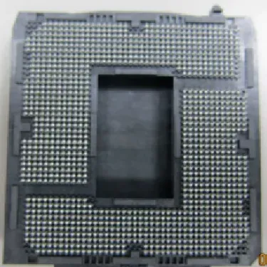
Figure 1 | CPU socket used in the affected assemblies
Production Information
The same socket was used across several products. Field data and in-factory records indicated each product exhibited a certain failure rate, averaging about 2%. The failure mode during functional test was Open.
Failure Analysis
Visual and Side-View Inspection
Visual inspection did not reveal bent or deformed contacts. Side-view inspection of the outer-row solder balls confirmed good solder wetting to the PCB pads with no evidence of pad offset or non-wet/open joints.
X-ray Inspection
Oblique X-ray at approximately 53° revealed a critical anomaly at the reported failing net positions:
- The solder ball was distinctly separated from the internal contact pin (gold pin) inside the socket, consistent with an electrical open.
- Subsequent checks on additional failing boards showed the same solder ball-to-pin separation at the corresponding locations.

Figure 2 | Oblique X-ray (≈53°) highlighting solder ball-to-pin separation at failing positions
Process Investigation
The failure distribution and key SMT process checks were examined to isolate the cause.
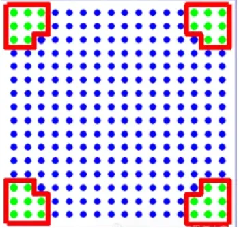
- Failure location mapping: Defects were distributed across corners and central areas rather than concentrated at edges. This pattern does not support edge-stress-induced solder cracking as the primary mechanism.
- Solder paste volume: X-ray suggested robust solder joints between solder balls and PCB pads, indicating no obvious solder volume shortage. To substantiate this, solder paste printing was reviewed: the stencil aperture ratio was 1:1.1 and SPI records showed no anomalies.
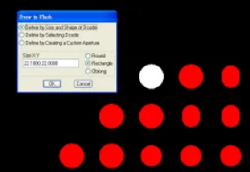
Figure 3 | SPI results confirming solder paste volumes within target (stencil aperture ratio 1:1.1)
- Reflow profile: Measured profiles were within the component specification envelope, and real-time oven temperature monitoring did not reveal abnormalities.
Date Code Correlation
All affected components traced back to the same date code. This correlation strengthened the hypothesis of a material- or lot-specific issue rather than a process drift.
Cross-Section (Microsection) Analysis
To support supplier engagement and root-cause confirmation, cross-sections were prepared from failing (NG) units. Several abnormal conditions were identified:
- Separation between the internal contact pin and the solder ball inside the socket.
- In some positions, the solder ball did not form a soldered connection to the PCB pad, likely due to non-coplanarity caused by the internal pin mechanically contacting the PCB during reflow.
- Contact pin intrusion up to the PCB solder mask, indicating interference with proper standoff.
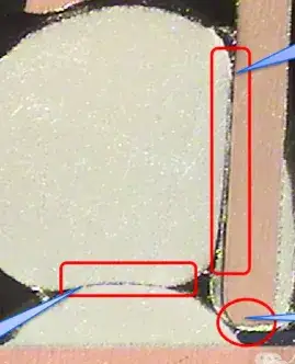
Figure 4 | Microsection from an NG unit: pin-to-PCB contact and ball-to-pin separation
Comparative cross-sections along the same row further illustrated clear differences in solder joint appearance between suspect and normal joints.
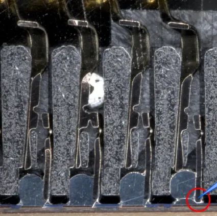
Figure 5 | Cross-row comparison: pronounced differences in joint morphology between NG and OK positions
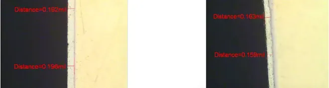
Dimensional measurements quantified the mechanical interference:
- NG joint: distance from the internal pin tip to the top-layer pad was 1.484 mil.
- OK joint: corresponding distance was 3.992 mil.
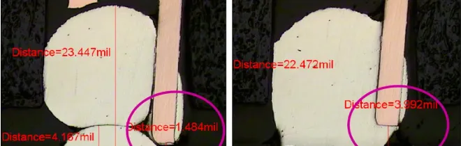
Figure 6 | Metrology: pin-to-pad distance of 1.484 mil (NG) versus 3.992 mil (OK)
Analysis Summary
The evidence converged on a lot-specific material nonconformance in the CPU socket. Variations in internal pin height or coplanarity caused the pin tip to contact the PCB solder mask during reflow, disturbing the intended standoff. This condition led to two failure manifestations: non-coplanarity preventing certain balls from properly wetting the PCB pad, and mechanical stress or inadequate engagement at the ball-to-pin interface resulting in internal separation. Process factors such as solder paste volume and reflow parameters were confirmed to be within control and not causal.
Corrective Actions and Verification
The supplier implemented material corrections on subsequent date codes to address pin height/coplanarity deviations. With the improved date code, a production run of 20,000 units showed no recurrence of the functional test open issue.
Mechanism and Engineering Lessons
CPU sockets that mount via an array of solder balls behave similarly to BGA components during reflow: collapse and standoff are governed by solder surface tension, ball geometry, pad metallization, and component coplanarity. However, sockets add another internal interface—the ball-to-contact-pin connection—that must remain mechanically and electrically intact through thermal excursion and post-reflow handling.
When internal pins protrude too far or lack coplanarity control, the pin tip can bottom out on the PCB solder mask or pad area during reflow. This premature mechanical stop interrupts normal solder ball collapse and alters local standoff. The resulting effects include:
- Non-coplanar balls that fail to reach and wet the pad, creating non-wet/open joints to the PCB even when paste volume is sufficient.
- Altered stress distribution through the ball and internal interfaces as the component is constrained by pin contact rather than by solder surface tension. This can fatigue or separate the ball-to-pin interface internally, yielding an open that is invisible to top-side visual inspection.
This case also illustrates the diagnostic value of oblique X-ray. Standard top-down X-ray often confirms voiding and gross bridging, but may miss internal separations within a socket. Tilting to around 45–60° provides parallax and contrast necessary to visualize the separation between the solder ball and the internal pin. Cross-sectioning then corroborates the internal condition and quantifies critical dimensions like pin-to-pad clearance.
Importantly, corroborating process health avoids false attribution to SMT parameters. SPI data with a 1:1.1 stencil aperture ratio, stable reflow profiles within the component’s thermal limits, and real-time oven monitoring collectively ruled out paste insufficiency or thermal misprocessing. The date code correlation made the material hypothesis testable and ultimately correct.
Recommendations for SMT and Incoming Quality
For high-reliability SMT assemblies that include sockets or packaged connectors with internal spring or pin structures, consider the following controls:
- Incoming inspection criteria for coplanarity and dimensional attributes directly related to standoff, including pin-to-bottom-surface height where specified by the supplier. Where practical, require data per date code.
- Oblique X-ray inspection during NPI or lot qualification to screen for internal ball-to-pin separation or abnormal standoff patterns not evident from top-down imaging.
- Targeted microsection sampling for first articles or when new date codes are introduced to establish baseline standoff and internal interface integrity.
- SMT baseline controls: maintain SPI limits aligned with stencil design (e.g., 1:1.1 aperture ratio when justified by pad geometry), verify reflow profile against component specifications, and monitor oven stability.
- Containment via date code traceability: if defects correlate to a specific date code, segregate inventory and coordinate with the supplier for corrective action and enhanced screening.
- Documentation of failure location maps across the array to distinguish process-driven edge effects from random lot-related distribution.
These measures help preempt recurrence of similar socket-related failure modes and accelerate root cause confirmation when issues arise.