Connectors are among the most common components encountered in electronics design and manufacturing. Their function is straightforward: they bridge interruptions in a circuit or connect otherwise isolated circuits so current can flow and the system can perform its intended functions. If you trace any signal or power path through an electronic product, you will typically find one or more connectors along the way. Connector types and mechanical structures vary widely depending on application, frequency, power level, and environmental conditions. Regardless of form factor, every connector must provide reliable, continuous conduction.
While "connector" often evokes electrical interconnect, the concept also extends to optical systems where light is the signal carrier and fiber replaces copper. Optical connectors serve a similar purpose—ensuring low-loss, reliable coupling. This article focuses on electrical connectors used in electronic circuits, with an emphasis on SMT-capable products and what process engineers need to understand about their construction and characteristics.
Why Use Connectors?
Without connectors, circuits would be permanently hardwired—typically through soldered connections—at every interface. Consider a vehicle battery: if the battery cables were permanently soldered to the terminals, assembly time and manufacturing cost would increase, and routine maintenance would be far more complicated. Replacing a worn battery would require desoldering in a service bay and soldering a new unit in place, incurring extra labor and downtime. With connectors, the process is simple: unplug, swap, and reconnect. This design approach improves manufacturability and serviceability, enhances flexibility during assembly and testing, and reduces total lifecycle cost.
Where Connectors Are Used
- Computers and peripherals: Mainframes, servers, workstations, PCs, and devices such as printers, modems, scanners, and external mass storage.
- Data communications and telecom: Networking equipment, telephony, wireless base stations, broadcast radio/TV equipment, and interconnect for copper and fiber systems.
- Consumer electronics: TVs, video players/recorders, audio systems, camcorders, and digital cameras.
- Automotive electrical and electronic systems: From safety and driver-assistance modules to body wiring harnesses, engine control, and transmission control.
- Other transportation and industrial: Aerospace, marine, military, and ruggedized equipment.
Connector Construction and Key Terms
Conductors and Connectors
At a basic level, a connector joins two open ends in a circuit so current can flow. The conductor is the physical path for current; it is often hidden within insulating or dielectric materials that allow multiple conductors to be routed in parallel without crosstalk or shorting. The most common conductors in interconnect systems are copper-based due to their balance of electrical, thermal, and mechanical properties. The image below lists commonly used conductors and their typical characteristics.
Basic Connector Elements
Connectors typically consist of a housing (also called an insulator or body), contact system, and mechanical features for polarization and retention. The diagram below illustrates typical terms used for these elements in an in-line connector, where conductors enter on one side and exit on the other. Mating halves are often referred to as the plug (male) and receptacle (female).
Housing (Insulator)
The connector housing provides:
- Mechanical support and accurate positioning of contacts (pins, receptacles, springs).
- Protection against dust, contaminants, and moisture.
- Electrical insulation between circuits and to the environment.
In addition to form factor, housings incorporate features for mating guidance, strain relief, latching, and keying to ensure correct assembly and robust operation.
Header (PCB-Mounted Base)
The connector half mounted on the printed circuit board is commonly called a header or base. Unlike an empty housing shell, a header integrates the contact pins or receptacles with the insulating body. Headers may be shrouded or unshrouded. Shrouding forms protective walls or skirts around the mating interface to improve guidance and robustness. Many headers incorporate friction-lock or latch mechanisms that enhance mechanical retention of the mated pair.
Headers are available in many geometries. Common variants include vertical (straight) and right-angle orientations, with single-row or multi-row pin grids to suit the required pin count and board layout.
Housing Plastics for SMT and Through-Hole
Housings are typically made from thermoplastics that can be melted and re-solidified, allowing efficient molding and recycling of sprues or runners. For reflow processes, the plastic must withstand elevated temperatures without deformation or degradation. Connectors intended for surface-mount technology (SMT) rely on solder terminations to pads on the PCB surface, whereas through-hole types (often called DIP) insert pins into plated-through holes and are subsequently soldered via wave or selective soldering, or are reflow-compatible with appropriate designs.
High-temperature thermoplastics are used for SMT-capable connectors to ensure dimensional stability and reliable solderability through reflow. The following image summarizes typical materials used for connector housings in high-temperature assembly environments.
Contact System: Terminals and Pins
The contact system creates the electrical interface within the mated pair and provides the PCB or cable termination on the rear side. Two primary types are commonly referenced:
- Terminals (receptacles, springs, blades, or crimp contacts) that mate with a corresponding pin and typically terminate to a wire or cable.
- Pins (posts) that mate into a receptacle and typically terminate to a PCB or cable assembly.
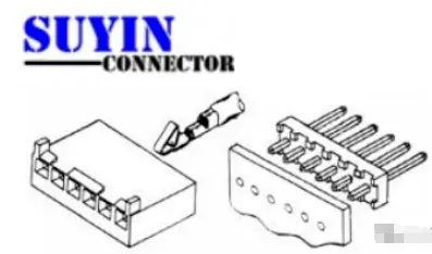
Each contact generally has two functional ends: the front mating interface that engages the corresponding contact in the opposite half, and the rear termination interface that connects to a conductor (e.g., via crimping, soldering, insulation displacement, or press-fit).
Base metal selection for the contact is critical. Copper alloys are widely used as the substrate due to their favorable blend of conductivity, thermal performance, elasticity, and formability. The image below summarizes commonly used contact base metals along with their advantages and tradeoffs.
Plating
Plating enhances electrical and mechanical performance of the contact interface. While base metals may offer strength and elasticity, they may not provide optimal corrosion resistance, wear resistance, or solderability. Strategic plating—either selective (only at the mating or solder areas) or overall—improves contact resistance, durability, and process performance. The following image outlines typical plating metals and their properties.
Polarization and Keying (Anti-Mis-mating)
Multi-pin connectors must ensure that each pin mates with the correct receptacle and that the halves cannot be reversed or misaligned. Polarization and keying features enforce a unique orientation and position during mating. Examples include asymmetrical shrouds, keys and keyways, and chamfered contact cavities that allow only one insertion direction. These features prevent assembly errors that could otherwise lead to circuit faults.
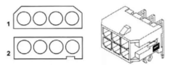
Circuit Identification and Pin Numbering
Clear pin numbering is essential for assembly, testing, and service. Common practices include a molded triangle indicating the numbering start position or an explicit "1" marking on the housing. These markings, along with PCB silkscreen indicators, help prevent wiring errors and facilitate troubleshooting.
Application Examples
Notebook Computers
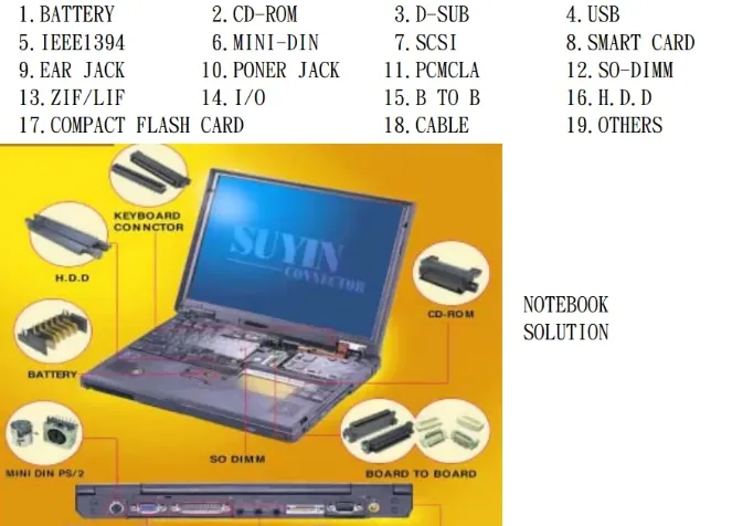
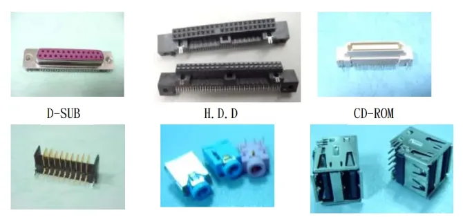
Notebook platforms integrate a variety of connectors for display interfaces, storage, keyboard and touchpad, battery and power, wireless modules, and high-speed I/O. Space constraints drive high-density, low-profile SMT connectors designed to survive reflow while maintaining mechanical robustness in thin housings.
Mobile Communication Devices
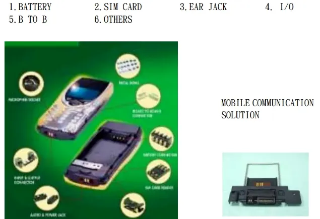
Smartphones and wireless modules use compact board-to-board, board-to-flex, and coaxial RF connectors. Requirements include precise impedance control for RF paths, high mating-cycle durability for test interfaces, and robust retention under drop and vibration conditions. Housing materials must be reflow-compatible and dimensionally stable to ensure consistent coplanarity and solder joint reliability on fine-pitch footprints.
Personal Computers and Boards
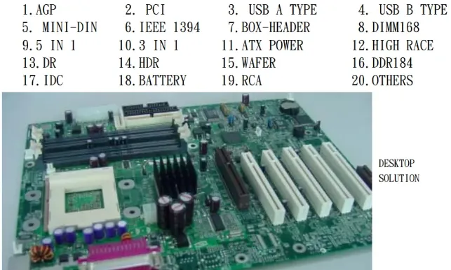
PC motherboards and add-in cards employ a wide variety of interconnects: power headers, high-speed serial connectors, memory sockets, storage connectors, and I/O interfaces. Designs balance signal integrity, mechanical stability, ease of assembly, and serviceability. Through-hole connectors remain common for high-insertion-force or mechanically stressed interfaces, often paired with reflow-soldered SMT components elsewhere on the assembly.
Process Considerations for SMT Connectors
For process engineers, several connector attributes directly affect manufacturability and reliability:
- Reflow capability: Housing material selection and contact retention design must tolerate peak temperatures and multiple heat cycles without warpage or loss of position, preserving true position and coplanarity.
- Plating and solderability: Termination plating stack-ups should provide stable wetting, controlled intermetallic growth, and reliable solder joints over the product’s storage life.
- Mechanical retention: Friction locks, latches, and shrouds help resist vibration, shock, and unmating forces during assembly and in the field.
- Polarization and marking: Clear keying and pin-one indicators reduce assembly errors and rework, especially in high-mix factories or manual plug-in operations.
- Cleaning and contamination control: Shrouds and housing geometry can reduce flux entrapment and ease cleaning, important for no-clean versus cleanable flux processes and for products requiring high insulation resistance.
By understanding how housing materials, contact base metals, plating, and mechanical features interact with PCB assembly processes such as reflow, wave, and selective soldering, process engineers can select connectors that meet both electrical performance and manufacturing robustness requirements.