This report documents a failure analysis performed on a power-module PCB assembly (PCBA), sample ID PCBA0228, focusing on metallographic cross-sections of specified solder joints, intermetallic compound (IMC) thickness measurements, plated through-hole (PTH) wall copper thickness, and external trace copper thickness. The investigation follows IPC-TM-650 sample preparation methodology and evaluates findings against IPC-A-610J (acceptability of electronic assemblies) and IPC-6012D (qualification and performance for rigid printed boards) Class 2 criteria.
1. Sample Description
The sample is a power board core assembly, quantity 1 piece, designated PCBA0228. The scope of work included:
- Metallographic cross-section analysis of specified solder joints.
- Measurement of IMC thickness at the hole wall/solder interface for selected component leads.
- Measurement of plated through-hole wall copper thickness.
- Measurement of external (surface) trace copper thickness.
Detailed sample information is summarized below.
Table 1 | Sample information
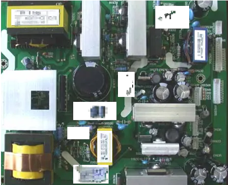
Figure 1 | Top-side appearance of the sample
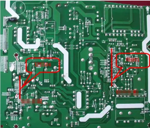
Figure 2 | Bottom-side appearance of the sample
2. Test Methodology
Sample preparation and analysis followed IPC-TM-650 2.1.1. The process was designed to preserve solder joint integrity while enabling accurate cross-sectional inspection and dimensional measurements.
Key steps:
- Sectioning: The PCBA area containing the specified components was cut from the assembly in a manner that avoids damaging the target solder joints.
- Mounting: The cut section was embedded in epoxy resin to provide mechanical stability during grinding and polishing.
- Grinding and polishing: The mounted sample was sequentially ground and polished until grinding scratches and contamination were removed, exposing a clean cross-section through the relevant solder joints, plated through-holes, and external traces.
- Etching and cleaning: The polished surface was etched and rinsed to reveal microstructural detail.
- Inspection and measurement: A metallographic microscope was used to examine overall solder joint structure, wetting, voiding, and interfaces. A scanning electron microscope (SEM) was then used to measure the IMC layer thickness at the solder/copper interface and to measure copper thickness on PTH walls and external traces.
The IMC layer of interest is the compound that forms between Sn-based solder and copper (e.g., Cu6Sn5 and Cu3Sn phases). Its thickness and morphology affect mechanical strength and long-term reliability. Through-hole wall copper thickness and external conductor thickness are critical for electrical performance, thermal behavior, and mechanical robustness, and are evaluated against IPC-6012D Class 2 requirements. Solder joint acceptability is assessed with IPC-A-610J Class 2 criteria.
3. Results and Observations
3.1 Metallographic Cross-Section Observations of Solder Joints
Cross-sectional analysis was performed for the specified solder joints. Representative summary results are shown below, followed by representative photomicrographs for two component locations (XPE004 and NE001).
Figure 3 | Representative metallographic photograph of XPE004 solder joint
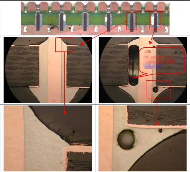
Figure 4 | Representative metallographic photograph of NE001 solder joint
Two leads were randomly selected for each of XPE004 and NE001 for IMC thickness measurements at the plated barrel wall/solder interface by SEM. Results are summarized below; representative SEM images follow.
Table | IMC thickness measurement results for selected pins of XPE004 and NE001
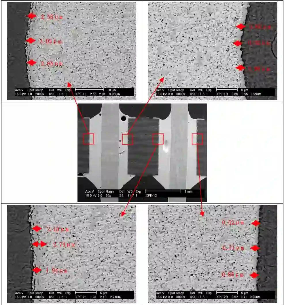
Figure 5 | Representative SEM image of XPE004 lead cross-section
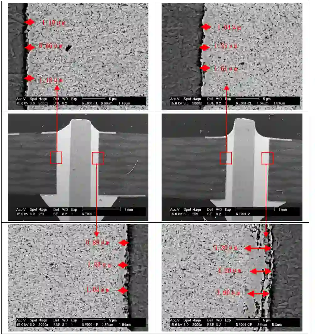
Figure 6 | Representative SEM image of NE001 lead cross-section
Engineering note on IMC: In Sn-based solder joints on copper, IMC forms at the interface, typically with a scalloped Cu6Sn5 layer and, under certain conditions, a thinner Cu3Sn layer adjacent to copper. IMC growth accelerates with temperature and time. Excessively thin IMC can be indicative of insufficient wetting or a weak metallurgical bond, while excessively thick IMC can embrittle the joint, increasing susceptibility to brittle fracture under thermal cycling or mechanical stress. Uniformity of the IMC along the hole wall is also important in PTH solder joints, as localized thin or thick regions can concentrate stress.
3.2 Through-Hole Wall Copper Thickness
Two plated through-holes on the sample were randomly selected for SEM measurement of copper thickness on the hole wall (barrel). Results are summarized below, with a representative SEM image.
Table 4 | Through-hole wall copper thickness measurement results
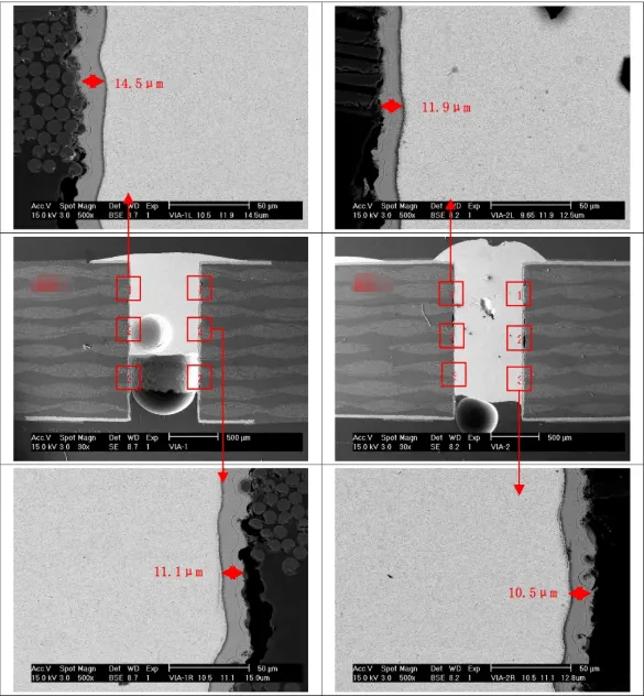
Figure 7 | Representative SEM image of a plated through-hole wall
Engineering significance: The PTH copper wall thickness directly affects current-carrying capacity, thermal conduction into the board stackup, and the mechanical integrity of the via barrel under thermal cycling and handling. Insufficient copper thickness can lead to higher I2R heating, degraded reliability in thermal shock, and a greater risk of barrel cracking, especially in high-aspect-ratio holes. Uniform plating around the circumference is critical; inadequate throwing power or non-uniform current density during electroplating can produce thin regions that govern reliability.
3.3 External Trace Copper Thickness
One wide and one narrow external trace were randomly selected for measurement of total external conductor thickness by SEM. The measurement locations and representative SEM views are shown below. According to IPC-6012D requirements for Class 2, when the base copper foil is 1 oz, the total thickness of the external conductor after plating shall be no less than 47.9 μm. The measured external trace copper thicknesses did not meet this requirement.
Engineering significance: External copper thickness influences current capacity, temperature rise, and, for high-frequency conductors, impedance and loss to a lesser extent via surface roughness and skin depth effects. Under-plated external copper reduces cross-sectional area and increases conductor resistance, which can cause elevated temperature rise in power paths, larger voltage drop, and reduced margin under peak load. On mechanically stressed boards, thinner copper also reduces peel strength and can increase the risk of trace damage during rework or field service.
4. Conclusions
- Against IPC-A-610J Class 2 acceptance criteria, the evaluated solder joints at XPE004 and NE001 were judged nonconforming.
- Against IPC-6012D Class 2 requirements, both the measured plated through-hole wall copper thickness and the measured external trace copper thickness were nonconforming.
Engineering Discussion and Corrective Considerations
While the measurements and accept/reject decisions are definitive for the inspected features, addressing root causes and preventing recurrence require a combination of PCB fabrication controls and SMT process optimization.
4.1 Solder Joint Integrity and IMC Control
- Wetting and barrel fill: For PTH component leads, adequate flux activation, correct solderability of finishes (component leads and PCB pads/barrels), and a thermal profile that ensures full barrel wetting are essential. Insufficient fill or localized voiding can correlate with non-uniform IMC formation and lower mechanical strength.
- Thermal profile optimization: Reflow or wave solder profiles should be validated to achieve the required time above liquidus and peak temperature consistent with solder paste or solder alloy specifications, avoiding both underheating (incomplete wetting, thin IMC) and overheating (excess IMC growth, interfacial embrittlement).
- Surface finishes and storage: Oxidation or contamination on copper or component leads impairs wetting and can produce erratic IMC morphology. Control of storage conditions, shelf life, and pre-cleaning where appropriate can improve consistency.
- IMC thickness management: IMC growth is time-temperature dependent. Process settings should seek sufficient metallurgical bonding without promoting excessive intermetallic growth. Long dwell or repeated rework cycles should be minimized.
4.2 Through-Hole Wall Copper Thickness
- Electroplating process control: Achieving compliant PTH wall copper thickness depends on plating bath chemistry, agitation, anode-to-cathode geometry, current density, and plating time. Monitoring throwing power and employing periodic test coupons can help ensure adequate and uniform deposition across the panel, including high-aspect-ratio holes and panel center regions.
- Design-for-manufacture (DFM): Hole aspect ratio, drill quality, desmear/activation uniformity, and via distribution influence plating uniformity. Collaboration with the PCB fabricator to set achievable aspect ratios and to optimize panel layout will improve conformance.
- Verification: Independent cross-sectional measurements and micro-resistance methods on coupons or sample holes can provide early detection of thinning trends before full production release.
4.3 External Trace Copper Thickness
- Base foil and plating targets: With a 1 oz base foil, the total external conductor thickness after plating must meet the stated IPC requirement. Fabricators should set plating targets above the minimum to cover process variation and etch-back effects, ensuring the final post-etch thickness meets specification.
- Uniformity across the panel: Current crowding can lead to over-plate near edges and under-plate in panel centers. Use of thieving patterns and balanced copper distribution can improve thickness uniformity and reduce localized thin regions.
- Electrical and thermal implications: For power circuitry, trace width and copper thickness work together to determine current carrying capacity and temperature rise. If thickness is below requirement, consider compensating with increased width where feasible, but the primary corrective action is to restore compliant plating.
4.4 Sampling and Acceptance Strategy
Because metallographic and SEM measurements are localized, sampling plans should be structured to capture worst-case features: smallest holes, highest aspect ratios, densest copper zones, and traces in thermally demanding nets. Where measurements approach but do not meet specification, process capability analysis and additional sampling are warranted to confirm systemic issues versus isolated defects.
In summary, the analyzed sample exhibited solder joints and copper thicknesses that do not comply with the referenced Class 2 requirements. The corrective path involves coordinated actions across soldering process control, PCB fabrication plating control, and DFM adjustments to ensure robust wetting, compliant IMC formation, and copper thicknesses that meet or exceed IPC-6012D Class 2.