During functional test (FCT), a high rate of contact failures was observed at the fan connector interface. In a production lot already in process, the defect rate reached approximately 80%. Preliminary process engineering analysis found a thin film-like contaminant covering the top surface of the CN2 fan connector pins. When this film was scraped away with a small blade, all previously failing units passed FCT, indicating a surface contact issue at the mating interface.
Under 50× magnification, the top ends of the CN2 pins showed a white, thin, film-like substance on the outer surface. A preliminary hypothesis was that the connector's tin plating reacted at elevated wave solder temperatures, locally depleting the plating and leaving a reaction product on the pin surface, which then led to poor contact during FCT.
1. EDX Composition Analysis of CN2 Pin Plating
Objective: Identify the plating composition on CN2 pins and check for evidence of flux residue.
Samples:
- Two CN2 connectors taken after standard wave soldering process.
- Two CN2 connectors from OK material (not wave-soldered).
Result: Energy-dispersive X-ray (EDX) analysis showed that the elemental composition of the plating was essentially the same between wave-soldered parts and OK parts. No carbon was detected on the wave-soldered pins, which rules out flux residue as the white film.
2. Assessment of Possible Flux Contamination
- For bottom-side (BOT) wave soldering, CN2 is a through-hole part located near the PCB top edge. The wave solder fixture incorporates side "wings" to prevent flux spray onto the upper side of the fixture.
- For top-side (TOP) wave soldering, the fixture includes a recessed protective "boss" around CN2 and uses clamping screws to seal the PCB tightly to the fixture, effectively preventing flux from wicking into the boss cavity.
Given the robust fixture protections and validated process parameters, flux ingress was considered unlikely. Additionally, the white film could not be removed with IPA, further excluding flux residue as its origin.
3. Plating Oxidation at Elevated Temperature
- Connector specification indicates tin-plated pins. Tin plating is prone to forming white metal oxides at elevated temperatures; stannous oxide formation is a plausible mechanism for a thin white surface film.
- Pins that had passed through the wave solder showed a white, thin film on the surface that could not be wiped off with IPA. These units tended to fail during FCT. Scraping off the film with a blade restored good contact and FCT pass.
- To isolate the effect of temperature alone, three connectors were mounted in a fixture and run through the wave solder machine twice without applying flux. The same white, film-like residue formed on the pin surfaces, consistent with oxidation rather than flux contamination.
4. Wave Solder Temperature Review
The top and bottom processes used the same wave solder settings. Both the setpoints and measured temperatures were reviewed, with the profile confirmed to meet the existing process configuration.
5. CN2 Pin Cross-Section Analysis
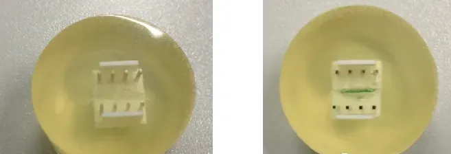
Objective: Measure post-process plating thickness and compare with non-processed OK parts.
Samples:
- CN2 connectors from the standard wave solder flow.
- OK connectors not subjected to wave soldering.
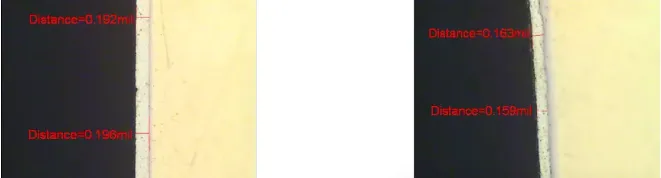
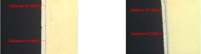
500× microscopy: The plating on the wave-soldered pins was visibly thinner than on the OK pins. This confirms that a chemical reaction occurred during the high-temperature process, consuming plating and generating other compounds on the surface.
6. Preliminary Conclusions from Root-Cause Screening
- Fixture protections around CN2 and EDX results make flux residue an unlikely cause of the white film.
- The white film cannot be removed with IPA, which also argues against flux residue.
- Cross-section analysis indicates plating thinning after high-temperature exposure, consistent with oxidation (e.g., stannous oxide formation) on tin-plated pins.
- Running parts through the wave solder twice without flux reproduced the same white, thin film on the pin surface as seen on failing units.
7. Immediate Corrective Actions and Planned Verification
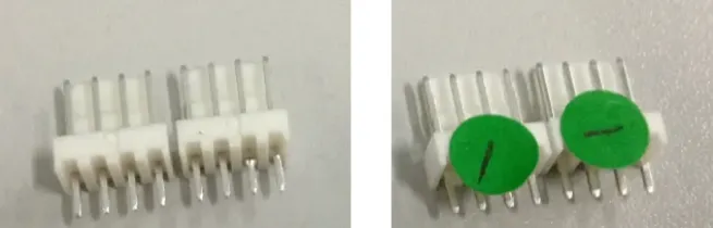
- As a temporary measure, apply high-temperature tape to cover the CN2 pin tips before DIP wave solder. Remove the tape after completing both top and bottom wave operations.
- Plan further verification across multiple fronts:
- Analyze plating behavior: run 20 connectors through a mini wave solder process and assess FCT results.
- Request 20 connectors with plating thickness at the upper end of the supplier's range (120–200 U) and evaluate after standard production.
- Confirm the tin finish type used on the pins (bright tin versus matte tin).
- Repeat cross-section to observe plating thickness changes after process exposure.
- Request 20 connectors with gold plating for trial production and evaluation.
8. Further Validation — Step 1: Procedure and Results
Procedure: Execute the planned step-by-step experiment to separate variables including tape masking, mini wave solder exposure, plating thickness variation, and material date code (D/C).
Initial findings:
- Based on quality records from PCBA supplier, mass production lots used material with D/C 20120619, so the impact of D/C could not be conclusively isolated at this stage.
- Masking CN2 with high-temperature tape during wave solder, then removing it after both sides were processed, substantially reduced the defect rate.
- Using thicker plating samples and running through the wave solder without other changes completely avoided the defect.
- Processing without tape on the mini wave solder line did not produce CN2 contact failures.
- The trial quantity was small, so additional data was required to select the optimal corrective path.
9. Further Validation — Step 2: Procedure and Results
Procedure:
- On November 29, introduce 100 pcs of special-supply material from the supplier (D/C: August 2012) into production without high-temperature tape masking. MO: 21491237. The stock material previously used had D/C 20120619.
- Run a separate order using 1,000 pcs of in-house stock (D/C: 20120619) with high-temperature tape masking. MO: 21491356.
Conclusions:
- The CN2 contact failure at the fan interface was not correlated with the material D/C.
- Special-supply material from the vendor did not improve the defect rate when processed without masking.
- Masking CN2 with high-temperature tape significantly reduced the defect rate but did not completely eliminate it.
- Proceed to a third experiment focused on plating finish modification to fully eliminate the failure mode.
10. Further Validation — Step 3: Plating Finish Change and Outcome
Procedure: To improve plating stability under high-temperature wave solder, request a change from bright tin to either matte tin or gold plating. The supplier selected gold plating at 1 U thickness and provided 100 pcs for trial production.
Result: In the 100-piece build with gold-plated pins, all units passed FCT with no test failures, demonstrating that an alternative, more oxidation-resistant finish at the mating interface can eliminate the contact issue.
Summary
The white, film-like residue on tin-plated fan connector pins after wave soldering caused intermittent or open contact during FCT. EDX composition analysis ruled out flux residue, and fixture design and IPA cleaning behavior further supported that conclusion. Cross-section microscopy showed plating thinning on wave-soldered pins versus OK parts, consistent with high-temperature oxidation of tin plating. Process experiments indicated that:
- Masking the mating portion of the pins with high-temperature tape reduces the defect rate by preventing thermal/chemical exposure of the contact area.
- Increasing tin plating thickness within the supplier's range can prevent the defect.
- Mini wave solder did not reproduce the failure in the limited sample set.
- Changing the plating finish to gold (1 U) eliminated the failure in a 100-piece validation run.
For mass production, either maintaining a robust masking process, increasing tin plating thickness, choosing a more oxidation-resistant plating (e.g., matte tin), or switching to a noble finish (e.g., gold) are viable paths to ensure stable contact performance through high-temperature wave soldering.