Abstract
As electronic products trend toward higher functionality and smaller size, component packaging has evolved accordingly. Traditional SOIC and TSOP packages are increasingly giving way to QFN (Quad Flat No-Lead) packages. A QFN typically features a large exposed thermal pad centered on the package underside that is soldered to a corresponding thermal pad on the PCB, delivering excellent electrical and thermal performance. The no-lead design reduces PCB real estate, and the very low impedance and low inductance make the package suitable for high-speed and microwave applications. These characteristics also raise the bar for manufacturability and reliability. In particular, when QFNs are used in PWM control circuits, the unique pad design can lead to short circuits among Vin, SW, and PGnd nets during reflow. To improve manufacturability and overall yield, process optimization must be aligned with the QFN package structure to enhance assembly welding yield and OATL.
Introduction
Due to the structural characteristics of QFN packages, improving soldering yield in mass production is a core goal for process engineers and manufacturers. Achieving this requires end-to-end process exploration and experimentation. By iteratively testing and collecting data, process parameters and stencil designs can be refined to improve overall assembly yield.
QFN Overview
A QFN is a square or rectangular no-lead package with a large exposed thermal pad located at the center of the package bottom. Electrical perimeter pads surround this thermal pad. The short conduction path from internal leads to external pads, together with low package inductance and low internal routing resistance, deliver excellent electrical performance. The exposed lead frame pad also provides a direct thermal path that efficiently dissipates heat from the die. QFN is a compact, plastic-encapsulated surface-mount package well suited to applications with stringent size, weight, and performance constraints.
In typical designs, the exposed thermal pad is soldered to a PCB land that may incorporate thermal vias, allowing heat to be conducted into large copper ground planes to absorb and spread thermal energy. Because of the small form factor, light weight, and strong electrical and thermal performance, QFN packages are widely used across power and RF applications.
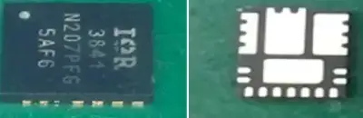
Figure 1 | QFN package with an exposed thermal pad soldered to the PCB
Soldering Challenges for QFNs with Exposed Thermal Pads
QFNs with a large exposed pad present recognized challenges in SMT. Achieving robust solder joints depends on a tightly controlled combination of placement parameters, stencil thickness and aperture design, solder paste particle size, and reflow profile. For high-power PWM control devices, the ground/thermal pad soldering must meet thermal and electrical requirements. The stencil aperture pattern and thickness, along with the solder paste powder type, strongly influence paste transfer efficiency, solder volume, wetting, voiding, and the risk of bridging.
Common failure modes on high-power PWM QFNs include bridging across fine-pitch perimeter pads, insufficient solder or poor wetting on the large thermal pad, and solder overflow from the exposed-pad region that leads to shorts between adjacent nets such as Vin, SW, and PGnd.
Case Study: Grounding Failure and Shorting Between Vin, SW, and PGnd
Background and Failure Mode
In a server power-supply application using an IR3841MTRPbF QFN package, the device features separate Vin, SW, and PGnd thermal/electrical pads. High thermal performance and reliable electrical conduction are required. During reflow, solder overflow on the Vin, SW, and PGnd exposed pads caused intermittent short circuits, resulting in functional failures and yield loss.
Process Conditions and Materials
The process conditions and materials used in verification were as follows:
- Lead-free solder paste: SAC387 alloy, Type 3 powder.
- Printing equipment: Panasonic SP28P-DH screen printer.
- Print parameters: squeegee speed 85 mm/s, squeegee pressure 28 N, separation speed 0.3 mm/s, separation distance 3.0 mm.
- Measured paste thickness: 0.15–0.17 mm with a steel squeegee.
Stencil Design Option 1 (Vendor-Style Aperture)
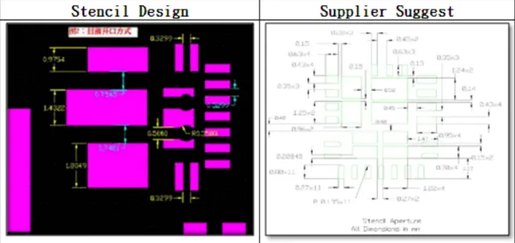
Option 1 followed the IC vendor’s general stencil guidance: perimeter apertures matched to pad size, and the exposed-pad apertures inset by 0.15 mm from the pad boundary.
Key device geometry in this design: the spacing between the Vin, SW, and PGnd exposed pads was 0.25–0.30 mm.
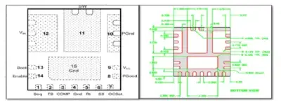
Figure 2 | Spacing between Vin, SW, and PGnd exposed pads: 0.25–0.30 mm
The stencil apertures under Option 1 and their relationship to the original footprint file are illustrated below.
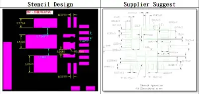
Figure 3 | Option 1 stencil apertures vs. original footprint
In Option 1, the exposed-pad stencil coverage was set above 80% of the pad area. Perimeter leads used rounded-corner apertures. The stencil area ratio was greater than 0.66, and the aspect ratio exceeded 1.66, meeting IPC-7525A recommendations.
However, reflow results showed that this approach was not feasible for the specific design. The exposed Vin, SW, and PGnd pads exhibited insufficient solder volume and wetting, with solder coverage on the exposed pads falling below 75%. At the same time, excess solder at the perimeter leads produced solder beads, failing customer quality requirements.
Stencil Design Option 2 (Modified Apertures)
Option 2 adjusted the stencil to mitigate solder overflow and improve exposed-pad wetting:
- On the SW exposed pad, the aperture edge was inset by an additional 0.1 mm relative to the adjacent pad edge to increase separation in the stencil pattern.
- Perimeter lead apertures were extended 0.15 mm outward in length to improve solder transfer and wetting on the leads.
- All other stencil parameters matched Option 1.
Verification showed that Option 2 achieved the required solderability and electrical performance. The revised apertures balanced solder volume on the large exposed pads and the fine-pitch leads, reduced the tendency for solder to migrate and bridge between adjacent nets, and eliminated solder-beading at the perimeter.
Practical Recommendations
- Based on repeated process trials, robust QFN solder joints depend on appropriate solder volume and aperture geometry. When solder coverage on the exposed pad is maintained around 80–85%, joints typically exhibit good wetting, reliable electrical conduction, and reduced risk of solder overflow that could lead to shorts.
- For QFNs where perimeter pads and the exposed thermal pad are closely coupled, avoid mesh-pattern apertures on the stencil for the exposed pad. During reflow, the solder on perimeter leads can be drawn inward toward the central exposed pad, resulting in insufficient solder on the leads. Using discrete, well-proportioned apertures aligned to the component pad geometry helps maintain proper solder distribution.
- When defining stencil apertures for exposed pads associated with different nets (for example, Vin, SW, PGnd), ensure adequate separation in the stencil design to prevent solder bridging. In this case, a safety spacing of at least 3.5 mm between stencil openings associated with different exposed pads was used to lower the risk of overflow-induced shorts.
By aligning stencil design with the specific QFN pad topology and spacing, and by selecting appropriate solder paste type, print thickness, and reflow conditions, manufacturers can improve solder wetting on large exposed pads while avoiding bridging on fine-pitch leads. The modified stencil approach demonstrated here resolved grounding failures and shorting between Vin, SW, and PGnd in a high-power PWM control application, meeting both functional and quality requirements while improving assembly yield.