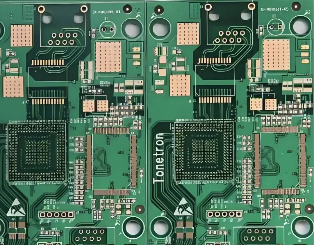
During routine SMT production, an 8-pin resistor array (resistor network, RP) exhibited misplacement and open-solder defects. One lot contained 20 defective units out of 760 (2.63%), and during the April 6 night shift on line D5, 18 units out of 800 (2.25%) were found with array offset and open solder. Cumulatively in March, 110 such defects had been recorded. This case study summarizes the cross-functional investigation, corrective actions, stencil design study, and the eventual stabilization of yield.
Initial Investigation and Suspected Causes
Preliminary checks focused on both placement and printing-related factors to isolate whether the defects originated from pick-and-place instability, incoming material variation, or solder paste transfer issues.
- Placement coordinates were verified to be correct.
- The component (part number 013-705000-000) was placed on a CM402-3 (318L) line. Part and machine settings were verified to be correctly configured.
- The taught pick-up position was verified. However, during feeding the pick-up location was observed to shift, even though the feeder itself was operating normally.
- Incoming material condition revealed a critical risk: the carrier tape pocket (cavity) was too wide. The component was able to rattle significantly in the pocket, allowing the part to be dragged or shifted during indexing and pick-up.

Dimensional checks then focused on the component and its carrier tape:
- Component body width: 1.00 ± 0.10 mm.
- Carrier tape pocket width specification: 1.20 ± 0.10 mm.
- Placement equipment vendor recommendation: pocket width should not exceed the component body width by more than approximately 20%, i.e., less than 1.20 mm.
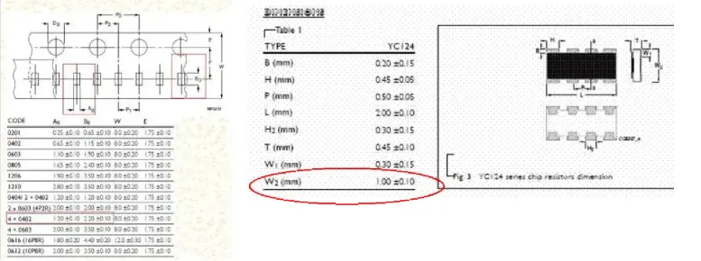
Using a coordinate measuring machine (CMM), the carrier tape pocket width was measured near the upper limit. While still within the component supplier's 1.20 ± 0.10 mm specification, it exceeded the placement equipment vendor's recommended maximum of 1.20 mm.
Corrective Actions and Interim Results
To stabilize placement and reduce mispick/misplacement related to excessive pocket clearance, the following actions were implemented:
- Requested the component vendor to ship lots with carrier tape pocket width strictly below 1.20 mm.
- Adjusted the placement feeder indexing speed from high to medium and instituted an in-process check of the pick-up position every 30 minutes during production.
These actions reduced the array offset defect rate significantly. Across the most recent four work orders, misplacement decreased to 3/2100 (0.1%). However, open solder defects (insufficient solder on some leads) still occurred, indicating that the dominant remaining failure mode was not solely placement-related.
Deeper Analysis: Solder Paste Printing and Stencil Design
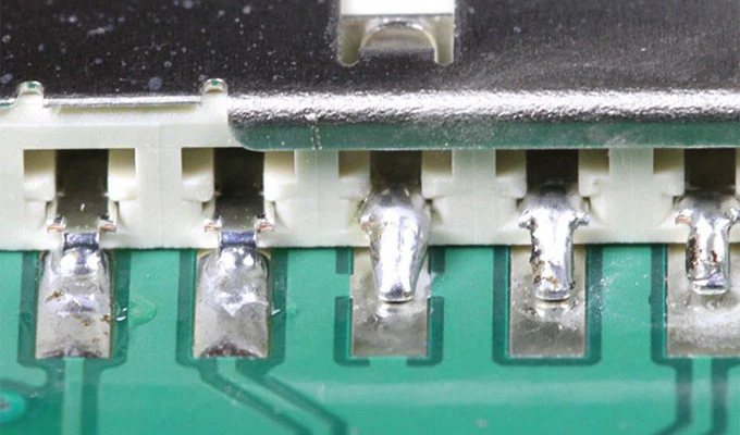
Failure analysis of NG samples revealed that the open solder tended to occur on the middle pins of the resistor array. Under magnification, the solder paste deposit on those pads was minimal, consistent with under-printing and poor paste transfer. Potential contributors included printer parameter settings, solder paste rheology (viscosity), the condition of the printer's under-stencil wipe system, and the stencil aperture design.
PCB Pad Layout and Stencil Parameters
The component is an 8-pin resistor array with 0.5 mm pitch. The middle pad design on the PCB was:
- L = 18 mil
- A = B = 8 mil
- D = 12 mil
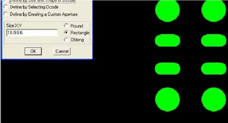
The stencil was 0.13 mm (5.1 mil) thick. The stencil vendor followed internal guidelines for aperture design. For the middle pads, the aperture length L1 remained at 18 mil, and the aperture width D1 was 8.6 mil.
Paste Release Metrics: Aspect Ratio and Area Ratio
SMT Stencil paste release is strongly tied to two geometric metrics:
- Aspect ratio = aperture width / stencil thickness. A typical target is greater than 1.5.
- Area ratio = aperture area / (aperture perimeter × stencil thickness). A typical target is greater than 0.66.
For the middle pad aperture:
- Aspect ratio = 8.6 mil / 5.1 mil = 1.68, which meets the common rule of >1.5.
- Area ratio = (18 mil × 8.6 mil) / {2 × (18 mil + 8.6 mil) × 5.1 mil} = 154.8 / 271.32 = 0.570, which is below 0.66 and indicates a higher risk of insufficient paste transfer and clogging during printing.
This explains why the middle pads were prone to under-depositing: although the aspect ratio passed, the area ratio was too low, making paste release difficult. Middle pads in tightly pitched arrays often face this issue because the required aperture dimensions to control bridging can drive the area ratio below the reliable transfer threshold, especially with a 5.1 mil stencil thickness.
Benchmarking and Aperture Optimization
Comparable products using similar arrays were reviewed to benchmark aperture strategies and solder volumes for the middle pads.
Based on the area ratio limitation, the stencil apertures for the middle pads were optimized to improve paste transfer while maintaining bridging margin between pads. The optimization increased the effective area ratio of the critical apertures and reduced the propensity for clogging and under-printing at the middle leads.
Production Result After Optimization
With the carrier tape pocket width managed, feeder speed moderated, in-process pick-up checks implemented, and the stencil aperture design optimized for improved paste release on the middle pads, the open-solder defect mode was eliminated. A subsequent production run of 2,000 boards recorded zero defects.
Why These Actions Worked
The improvements addressed both the mechanical stability of placement and the physics of paste transfer:
- Carrier tape pocket width: Excessive clearance allows the part to sit off-center or rotate within the pocket. During feeder indexing, this increases pick-up eccentricity, nozzle correction burden, and XY/θ misplacement risk. Tightening the pocket width within the placement vendor's recommendation reduced positional variability at the moment of pick-up.
- Feeder speed and pick-up verification: Reducing indexing speed lowered impulse forces on the part in the pocket, while frequent pick-up checks caught progressive drift due to tape lot variation, nozzle wear, or feeder indexing tolerance.
- Stencil area ratio: The dominant remaining failure mode was insufficient solder on middle pads. Although the aspect ratio was adequate, the area ratio was below the reliable release threshold. Adjusting aperture geometry to increase the effective area ratio improved transfer efficiency, especially critical on inner apertures that tend to clog first and suffer from lower wipe efficacy.
- Printer process variables: While not the primary root cause in this case, maintaining proper squeegee pressure and speed, paste roll height, wipe frequency, and paste rheology supports consistent aperture filling and release. These parameters were verified and controlled to complement the stencil improvements.
Key Takeaways for SMT of Fine-Pitch Resistor Arrays
- Control incoming carrier tape pocket width relative to component body width. Excessive pocket clearance is a frequent root cause of pick instability, misplacement, and intermittent open solder due to poor lead-to-paste contact on the board.
- Use in-process checks for pick-up position on susceptible components. Periodic verification helps detect drift caused by lot-to-lot tape variation or gradual equipment changes.
- Evaluate stencil apertures using both aspect ratio and area ratio. Passing the aspect ratio alone does not guarantee reliable paste transfer; area ratio below about 0.66 correlates strongly with under-depositing and clogging.
- When area ratio is marginal on middle pads, adjust aperture geometry to raise effective area ratio while controlling bridging. Coordinate thickness selection, aperture sizing, and printer settings as a system.
- Correlate failure locations with specific physical mechanisms. In this case, open solder on middle pads pointed directly to printing and paste transfer, which guided the stencil optimization.
By systematically addressing tape pocket tolerance, feeder dynamics, pick verification, and stencil aperture design, the process transitioned from sporadic misplacement and open solder to stable, defect-free production.