In modern electronics manufacturing, wave soldering remains a core interconnection process for through-hole (THT) and mixed-technology (SMT + THT) assemblies. Its stability directly determines product reliability, service life, and competitiveness. Despite increasing automation, defects such as non-wetting, bridging, and poor through-hole fill still occur frequently, hurting yield. Among many contributing factors, flux is often treated as a secondary consumable—but in practice it plays a central role. Flux governs surface cleanliness, wetting dynamics, heat transfer efficiency, and post-soldering reliability.
This article consolidates engineering documentation and shop-floor experience to map the full lifecycle mechanisms of flux in wave soldering, analyze flux-driven defect mechanisms, and propose a practical evaluation and selection framework for high-performance fluxes. The goal is to provide process engineers and manufacturing teams with a technically rigorous and actionable reference to improve weld quality, reduce rework, and support greener manufacturing.
Four Common Wave Soldering Defects Driven by Flux and Their Mechanisms
Many defects that appear to stem from machine settings or operator error ultimately trace back to flux selection, insufficient activity, uneven coverage, or poor thermal stability. The following sections examine four frequent issues: non-wetting, poor through-hole fill, bridging and icicles, and board cleanliness problems.
1. Cold Solder Joints (Non-Wetting): Surface Condition vs. Chemical Activity
Non-wetting is one of the most insidious and damaging defects in wave soldering. It manifests as poor metallurgical bonding between solder and base metal, large contact angles, and spherical or discontinuous solder deposits. The root cause is a "barrier layer" on the metal—primarily oxides, sulfides, or carbides—that prevents wetting.
Metals spontaneously form oxide films in air. Even copper, with generally good solderability, readily forms Cu2O or CuO at the surface. These non-metallic corrosion products behave like an insulating layer that prevents liquid solder from contacting clean metal atoms. Heating and solder flow alone cannot overcome this barrier.
One of the core functions of flux is to remove these oxide films. If flux activity is inadequate, it cannot effectively decompose or dissolve the oxides. Historically, before the 1960s, Chinese military production commonly used rosin–alcohol fluxes with inherently weak chemical activity, and non-wetting was rampant. When missile radar production lines were later introduced from the Soviet Union, a classified, high-performance flux formulation was specifically provided—underscoring the criticality of flux chemistry.
Even today, many high-reliability military manufacturers prefer mildly activated rosin (RMA) flux paired with rigorous cleaning rather than lower-activity no-clean fluxes, in order to minimize non-wetting risk and guarantee long-term stability in harsh environments. For components or PCBs with marginal solderability, fluxes with sufficient activity must be used to fully clean metal surfaces during preheat and solder contact.
2. Poor Through-Hole Fill (Solder Starvation): Spreadability and Application Method
Through-hole fill quality is a key indicator of wave soldering performance. Ideally, solder should rise from the bottom side to the top side of the PCB, forming full fillets. In practice, incomplete fill, one-sided wetting, or partial voiding occurs frequently.
When PCB and lead solderability are confirmed (for example, wetting balance zero-crossing time below 1 s), and wave height, conveyor speed, and board angle are appropriately set, persistent poor fill often points to flux issues:
- Poor spreadability
Flux must exhibit excellent wetting and spreading to draw solder into narrow holes. Excessive viscosity or high surface tension limits penetration along plated barrel walls, preventing solder rise.
- Insufficient activity
Plated through holes (PTHs) are confined spaces with limited air exchange. While oxidation may proceed more slowly, surface cleaning is harder. Flux with inadequate activity will not remove trace oxides inside the barrel, degrading wetting.
- Application method
Spray fluxing is susceptible to component "shadowing," which prevents flux from entering holes, causing poor fill. By contrast, foam fluxing can deliver flux more uniformly into holes, as bubble rupture and recirculation improve coverage.
For dense PCBs with many PTHs, select low-viscosity, high-spreadability flux and optimize application. Increasing preheat temperature can further reduce viscosity and improve flow into holes.
3. Bridging and Icicles: Oxidation and Flux Depletion in the Peeling Zone
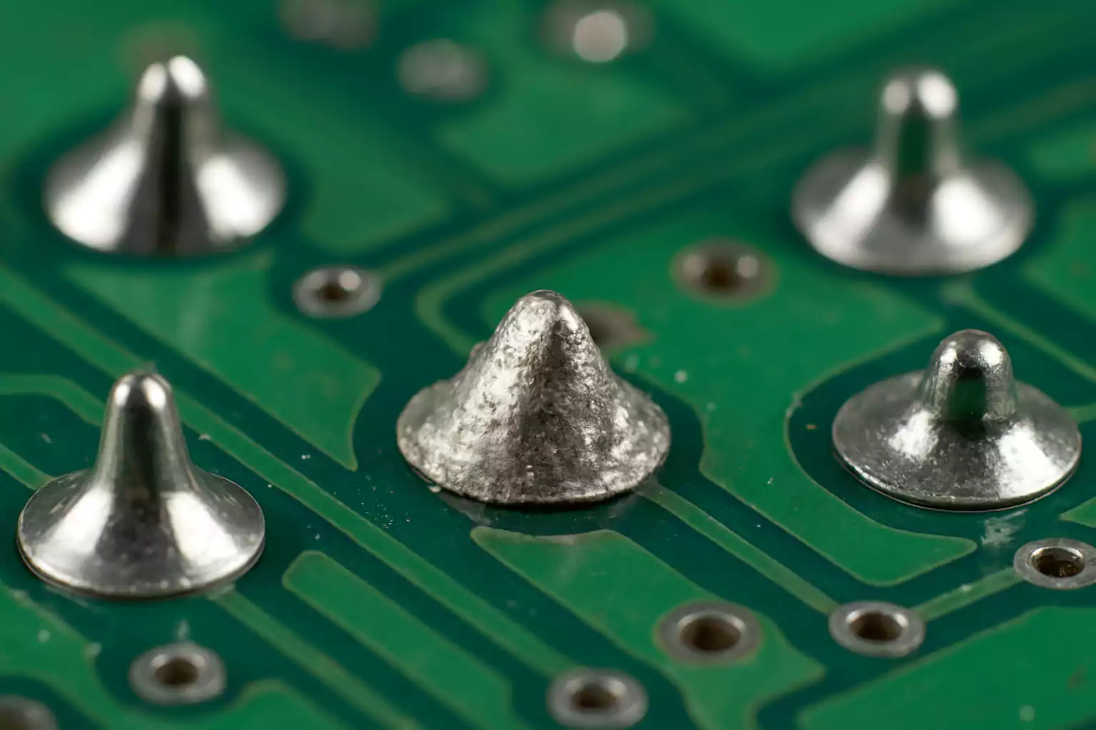
Bridging (excess solder connecting adjacent pins) and icicles (sharp tails of solidified solder) not only degrade appearance but create short-circuit risk. While excessive wave height, slow conveyor speed, or large board angle can contribute, flux behavior in the peeling zone is equally critical.
As the PCB exits the wave, the liquid solder detaches from the board. If flux maintains a protective film on the solder surface at this instant, it limits air exposure, suppresses oxidation, and allows surface tension to contract the solder smoothly—preventing tails or bridges. If flux decomposes at high temperature or is largely washed away by the first wave in a dual-wave system, the solder surface oxidizes rapidly during peeling, loses mobility, and tends to form.
- Bridging
Oxide films impede solder runoff, leaving excess solder between adjacent pins.
- Icicles
Oxidized solder cannot detach smoothly before solidifying, forming sharp protrusions.
A representative case: two capacitors with only 0.63 mm spacing (less than the typical 1.27 mm) created a high-density layout. With a new nozzle and dual-wave soldering, bridging occurred almost 100% at two sites, while switching to a single wave (only the second wave active) dramatically reduced bridging. In the dual-wave process, the board's flux was largely consumed by the first wave, leaving insufficient flux to protect the solder surface in the peeling zone at the second wave. Oxidation increased, fluidity deteriorated, and bridging resulted. In multi-wave systems, flux thermal stability and retained activity are essential.
4. Board Cleanliness and Reliability Risks: Electrochemical Effects of Residues
As products become smaller and denser, post-solder cleanliness has a direct impact on long-term reliability. Flux chemistry, solids content, and decomposition behavior determine the nature of residues:
- Ionic residues
Halides or organic acids that do not fully decompose can ionize in humid environments and form micro-galvanic cells. This drives electrochemical migration (ECM), increasing leakage and even causing shorts.
- White residues
Common with some no-clean fluxes, often rosin- or polymer-based. While not necessarily conductive, they impair appearance and can interfere with conformal coating.
- Particulates and carbonized deposits
At high temperatures, flux can carbonize or form insoluble salts with metals, creating black spots or particles that degrade insulation performance.
Flux selection is a balance between activity and cleanliness. Highly active fluxes improve first-pass yield but can compromise reliability if residues are corrosive. No-clean fluxes minimize residues and support environmentally friendly processes but require tight control of the process window.
Five Core Mechanisms of Flux in Wave Soldering
From a physical chemistry perspective, flux is not simply a "cleaner." It is a multifunctional medium that acts from preheat through wave contact to cooling and peeling.
1. Removing Oxide Films: Two Chemical Paths
Oxide films are not removed by simple solvent action; they must be converted to soluble compounds or reduced to pure metal. Two primary mechanisms are used:
- Complexation and dissolution
Rosin-based fluxes contain abietic acid and related resin acids that react with copper oxides (e.g., CuO) at elevated temperature to form copper abietates. These products dissolve in alcohols (e.g., IPA) and are carried away or encapsulated, exposing clean copper. This is non-corrosive to the base metal.
- Reduction
Specialized fluxes or reducing atmospheres such as hydrogen can reduce metal oxides according to MO + H2 → M + H2O. At high temperature, oxides are reduced to metal, water vapor escapes, and no residues remain.
2. Preventing Reoxidation: Forming a Thermal Protection Barrier
Wave soldering subjects the PCB to preheat above 100 °C and solder contact near 250 °C. Elevated temperatures accelerate reoxidation. Flux must form a continuous liquid or vapor film on surfaces during heating to exclude oxygen, especially critical in the peeling stage: if the solder surface oxidizes before wave exit, robust joints cannot form.
3. Lowering Liquid Solder Surface Tension: Managing Wetting Dynamics
Wetting underlies soldering. According to Young's equation, the contact angle θ depends on the balance of solid–vapor (γSV), liquid–vapor (γLV), and solid–liquid (γSL) interfacial energies: cosθ = (γSV ? γSL) / γLV. Good wetting (θ < 90°) requires increasing γSV or decreasing γLV and γSL.
Flux optimizes interfacial energy by:
- Removing oxides and restoring high surface energy (γSV) of the base metal.
- Forming an interfacial layer on liquid solder that significantly lowers γLV.
- Improving solid–liquid bonding to reduce γSL.
Additionally, "secondary spreading" occurs when viscous, preheated flux encounters the hot wave and its viscosity drops sharply. The rapid flow exerts shear that drags molten solder, further promoting spread.
4. Acting as a Heat-Transfer Medium: Eliminating Insulating Voids
In THT soldering, micro-gaps exist between leads and PTH walls. Air trapped in these gaps is a poor thermal conductor. Without flux to displace air, this "insulating layer" impedes heat transfer into the joint, causing cold joints or intermittent wetting. As a liquid, flux fills these gaps, replaces air, and enables efficient heat transfer to quickly reach thermal equilibrium and complete solder melting and wetting.
5. Promoting Molten Solder Flow: Momentum Transfer and Capillary Assistance
At the wave crest, the board and solder are in relative motion. Under high temperature, flux undergoes vigorous secondary spreading. The high-velocity liquid film imparts additional drag on the solder, helping it overcome gravity and surface tension and flow into higher or tighter regions. This is especially important for PTH "hole fill" performance.
Flux Types: Operating Modes and Application Scenarios
Fluxes have evolved from simple rosin to activated rosin, water-soluble, and no-clean formulations. Their distinct physicochemical behaviors must be matched to product requirements.
1. Rosin-Based Flux
- Mechanism
Predominantly resin acids in alcohol solvents; oxides are removed by forming soluble metal abietates.
- Characteristics
Moderate activity, good film-forming residue with some insulating properties.
- Use cases
General consumer electronics; halogen control recommended.
2. RMA (Rosin Mildly Activated)
- Mechanism
Organic acids or amine activators are added to rosin to boost deoxidation capability.
- Characteristics
Strong soldering capability, significantly reduces non-wetting; residues may be ionic—cleaning required.
- Use cases
High-reliability equipment (mil/aero) where corrosive residues are unacceptable.
3. No-Clean Flux
- Mechanism
High-boiling solvents with low solids content; active species are designed to volatilize or decompose at soldering temperatures, leaving inert polymeric residues.
- Characteristics
Negligible residue or faint white powder; no post-cleaning, supports environmentally friendly, high-throughput production.
- Process window
Typical settings: board preheat 95–130 °C, solder pot 235–275 °C, and contact time around 4 s. Too low, and activity is not fully activated; too high, and carbonization can occur.
- Use cases
Consumer electronics and communications equipment prioritizing efficiency and green manufacturing.
A Scientific Framework for Flux Performance Evaluation and Acceptance
To ensure robust soldering, organizations should institute a complete evaluation flow from supplier documentation through in-house validation, covering both static indices and dynamic on-machine testing.
1. Supplier Capability Dossier: Physical/Chemical and Application Data
Each lot of flux should be accompanied by two core data sheets for quality traceability:
- Table 1: Physical and Chemical Indicators
- Appearance and color
- Density (g/cm3)
- Solids content (%)
- Acid value (mg KOH/g)
- Halogen content (Cl, Br, I)
- Water-extract resistivity (Ω·cm)
- Copper mirror corrosion test result
- Table 2: Application Process Data
- Recommended preheat temperature range (°C)
- Applicable solder pot temperature (°C)
- Recommended application rate (ml/m2)
- Foam height or spray parameters
- Conveyor speed (cm/min)
- Material Safety Data Sheet (MSDS)
2. On-Machine Validation Tests
Datasheets cannot fully predict production behavior; machine trials are mandatory. Recommended checks include:
- Through-hole fill
Use a standard test board with multiple PTH diameters and verify ≥75% fill (IPC-A-610H).
- Defect rate statistics
Run at least 10 consecutive panels, recording non-wetting, bridging, icicles, etc. Target ≥99% yield.
- Board surface cleanliness
- Visual: no obvious residues, whitening, or carbonized spots.
- ROSE ionic contamination: residues should be < 1.5–5.0 μg NaCl/cm2.
- SIR: > 2 × 10? Ω-cm to mitigate electrochemical migration risk.
- Reliability screening
As needed, perform thermal cycling and damp heat aging to observe joint strength and electrical drift.
Conclusion: Toward High-Reliability, Greener Wave Soldering
Flux is small in volume but central to process outcomes. It is the enabler of metal-to-metal joining, a thermal conduit, an oxidation shield, and a flow guide. As manufacturing pushes toward higher density, reliability, and sustainability, flux must be treated as a core process variable rather than a generic consumable.
For high-reliability products, prefer sufficiently active, cleanable fluxes to eliminate non-wetting risk. For consumer products, adopt no-clean flux where appropriate, but rigorously maintain its process window to prevent under- or over-processing.
Looking ahead, with continued trends in lead-free alloys and miniaturization, fluxes will evolve toward lower residues, higher thermal stability, and wider process windows. A deep understanding of flux mechanisms coupled with a disciplined evaluation framework enables the transition from "it solders" to "it solders well" to "it is dependable."
Appendix: Flux Selection and Troubleshooting Cheat Sheet
| Defect | Likely Cause | Recommended Action |
|---|---|---|
| Non-wetting / cold joint | Insufficient flux activity | Switch to RMA or a formulation with stronger activators |
| Poor through-hole fill | Poor spreadability, uneven coverage | Optimize spray parameters, consider foam fluxing, increase preheat |
| Bridging / icicles | Unprotected peeling zone, flux depletion | Review wave sequence; ensure adequate flux coverage at the second wave |
| White surface / corrosion | Hygroscopic, high-ionic residues | Enforce cleaning or move to no-clean; control application volume |
| Poor thermal stability | Carbonization at high temperature | Lower preheat; select a high-thermal-stability formulation |
By applying a rigorous, mechanism-based approach to flux selection and control, engineering teams can treat wave soldering as a predictable, high-yield process and elevate overall manufacturing performance.