1. Fundamentals of C-SAM Technology
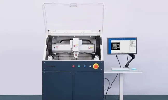
C-SAM, commonly referred to as C-mode scanning acoustic microscopy, is an advanced non-destructive inspection technique.
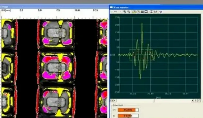
Its operating principle leverages the propagation behavior of ultrasound in different media. As an ultrasonic wave travels through a material, it encounters interfaces where density, elastic modulus, or other acoustic properties change. At each such interface, part of the wave is reflected and part is transmitted. C-SAM emits focused ultrasound, receives the echoes returning from internal interfaces, and processes the time-of-flight and amplitude information to reconstruct internal structure and detect defects.
C-SAM offers several notable advantages. First, it is non-destructive, so it does not damage the sample—critical for high-value, irreplaceable, or qualification units. Second, it achieves very high resolution, down to the micrometer scale and in favorable cases approaching sub-micrometer features, making it possible to locate subtle defects and structural anomalies. Third, it detects a wide range of defect types—such as delamination, cracks, and voids—across many package and substrate constructions. It is also non-contact, which avoids surface contamination or mechanical damage during inspection.
Because of these characteristics and its layer-specific imaging capability, C-SAM plays a key role in electronics packaging and materials engineering, helping teams characterize internal interfaces and ensure product quality and reliability.
2. Key C-SAM Application Areas in SMT
2.1 Electronic components
In SMT assembly, component quality is paramount. C-SAM is widely used to detect internal delamination, cracks, and voids within electronic components. High-frequency acoustic scanning can capture subtle yet performance-critical anomalies at material interfaces. For integrated circuits, for example, C-SAM can reveal internal structural issues such as die attach voiding or delamination between die, adhesive, and molding compound, enabling corrective action before functional reliability is compromised.
2.2 LEDs
For LED products assembled via SMT, C-SAM is particularly valuable. It can detect package delamination, cracks at the chip-to-substrate interface, and trapped voids in the encapsulant or die attach. If left unaddressed, these defects can lead to non-uniform emission, reduced luminous output, thermal stress concentration, and even catastrophic failure. Screening and root-cause analysis with C-SAM support higher yields and stable optical performance.
2.3 Metal-core substrates
Metal-core substrates are frequently used as carriers for thermally demanding assemblies. C-SAM identifies delamination in plating or coating layers, internal cracks, and voids in the substrate stack. Such defects may originate in manufacturing or be induced in service, degrading thermal conduction and electrical integrity, with cascading effects on overall system stability and reliability.
Across electronic components, LEDs, and metal-core substrates, C-SAM improves quality assurance in SMT, reduces scrap and rework, and supports continuous process improvement in electronics manufacturing.
3. Advantages of C-SAM for SMT Process Control
3.1 Precise layer and depth localization
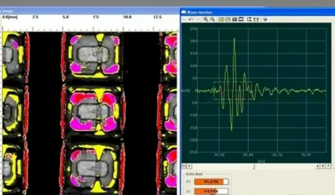
One of C-SAM's defining strengths is its ability to localize defects to a specific layer and depth. While X-ray imaging can reveal voids and cracks, it often struggles to unambiguously assign the defect to a particular internal interface. C-SAM, by contrast, provides clear time-of-flight and amplitude signatures for echoes from distinct layers, allowing engineers to identify the exact interface and depth at which a delamination, crack, or void resides. This layer-specific mapping makes corrective actions more targeted and effective.
3.2 High sensitivity to planar interface discontinuities
C-SAM is especially sensitive to discontinuities at relatively flat, planar interfaces. Subtle gaps, micro-cracks, or partial delamination that can be overlooked or misinterpreted by other methods are often readily detected acoustically because the impedance mismatch at an air gap or separation produces a strong reflection. This sensitivity improves detection accuracy and reduces the risk of false negatives when analyzing adhesive bonds, die attach layers, and encapsulated interfaces.
3.3 Excellent for delamination analysis in plastic packages
In plastic-encapsulated devices, C-SAM excels at detecting and characterizing delamination. It can visualize the location, lateral extent, and severity of separations between the molding compound and adjacent surfaces such as die, die paddle, and leadframe. Many alternative methods are less effective or more difficult to apply to fully encapsulated components, making acoustic microscopy a preferred technique during failure analysis, incoming inspection, and process qualification.
These strengths make C-SAM an indispensable tool for SMT process control—enabling early detection of internal defects, reducing defect escape, and supporting higher productivity.
4. Case Studies
4.1 Failure analysis of surface-mount MOSFETs
In production, it is not unusual to encounter lots of surface-mount MOSFETs that pass electrical test at the component level but exhibit a high rate of electrical failures after SMT assembly—such as drain-to-source leakage or short circuits—with failure rates exceeding 50% in severe cases.
A plausible analysis path is to consider the package construction and assembly stress. Large die area in a given package style raises sensitivity to moisture exposure and hermeticity, and increases the risk of stress mismatch during reflow. To validate this, the analysis can replicate SMT conditions on devices from the same package lot and use C-SAM to scan for delamination.
Sampling devices after simulated SMT reflow and scanning them acoustically revealed significant delamination between the die attach pad area (PAD) and the molding compound. Subsequent destructive analysis of failed units showed die cracking inside the package.
This case demonstrates the accuracy and effectiveness of C-SAM for detecting delamination and internal cracking in surface-mount MOSFETs. Early identification of these issues enables manufacturers to refine packaging processes, select more suitable materials, and optimize assembly profiles, thereby reducing field and production failures and improving long-term reliability.
4.2 Additional applications
Beyond MOSFETs, C-SAM is broadly applied across SMT processes for electronic components, LEDs, and metal-core substrates. For semiconductor devices, acoustic scans have revealed subtle internal delamination that prompted timely process adjustments and prevented downstream quality escapes. In LED assembly, C-SAM has identified interface cracks between the chip and substrate, allowing screening and rework to improve yield and uniformity. On metal-core substrates, detection of plating delamination and internal cracking has guided process optimization and enhanced thermal and mechanical performance.
These examples further illustrate C-SAM's critical role and broad value in SMT manufacturing.
5. Outlook for C-SAM in SMT
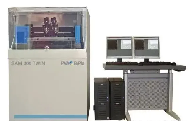
5.1 Technical improvement directions
As SMT technology advances, C-SAM is poised to improve in several areas. Resolution may be further enhanced to detect smaller defects and finer structural anomalies, driven by transducer optimization, improved signal processing algorithms, and higher-performance acoustic lenses. Capability for complex materials and multilayer stacks is likely to expand, enabling more accurate discrimination of defects in composite and highly integrated constructions. Throughput will continue to improve via faster scanning mechanisms and parallelized data processing to keep pace with high-volume manufacturing. Lowering inspection cost through reduced capital expense, simpler maintenance, and longer system lifetime is also an important direction.
5.2 Broader application prospects
Demand for C-SAM will grow as electronics continue to miniaturize and adopt higher-density packaging, increasing the need to detect small-scale defects in densely integrated assemblies. In new energy applications such as electric-vehicle control systems, C-SAM can help verify the integrity of critical components. In medical-device manufacturing, where high precision and reliability are essential, acoustic microscopy will play an important role in quality assurance. The rollout of 5G and advanced communications places tighter demands on inspection technologies; C-SAM is well positioned to support these requirements. In addition, integrating C-SAM with complementary inspection modalities can yield more comprehensive diagnostics and more efficient inspection workflows, further strengthening SMT process control.