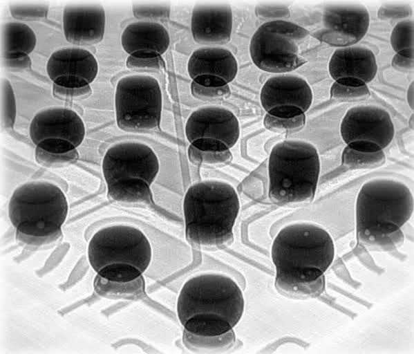
Reworking a BGA (ball grid array) device is inherently challenging. When the area beneath a BGA is densely populated—especially with large components—the difficulty and risk go up sharply. Large components under the device interfere with uniform heating of the solder joints during removal and replacement, and they are themselves exposed to bottom-side preheat and hot air, which can damage parts or cause them to drop off. To balance layout needs with reworkability, a clear set of design-for-manufacturability (DFM) rules is essential.
This article presents a practical DFM rule set for keeping the bottom side under BGAs clear of large parts and for maintaining sensible same-side clearance around BGAs, along with the engineering rationale and a straightforward verification method designers can apply before release to manufacturing.
DFM Rules for BGA Reworkability
For any component likely to require BGA-style rework equipment—such as BGAs themselves, CPU sockets, QFNs/LGAs, and long SMT connectors—apply the following two rules in PCB layout.
1. Bottom-Side Restriction
-
Requirement: On the PCB bottom side directly under the BGA footprint, do not place any component larger than 3216 (imperial) or 3225 (metric).
-
Plain-language interpretation: Under the BGA on the back of the board, only small "chip-size" passives like 0402, 0603, or 0805 are acceptable. Do not place large components—such as electrolytic capacitors or power inductors—of 3216 and above in that projected area.
2. Same-Side Clearance
Maintain the following minimum clearances on the same side of the PCB between the BGA and adjacent components. Measure from the outer edge of the body or pad, whichever is closer:
| Adjacent component type | Minimum clearance | Notes |
|---|---|---|
| BGA vs DIP through-hole | 4 mm | Clear DIP leads and avoid wave-solder impacts during rework |
| BGA vs BGA / tall parts (> 2 mm) | 2 mm | Includes connectors, tall ICs, heat sinks, etc. |
| BGA vs low-profile parts (≤ 2 mm) | 1 mm | Typical chip resistors and capacitors |
-
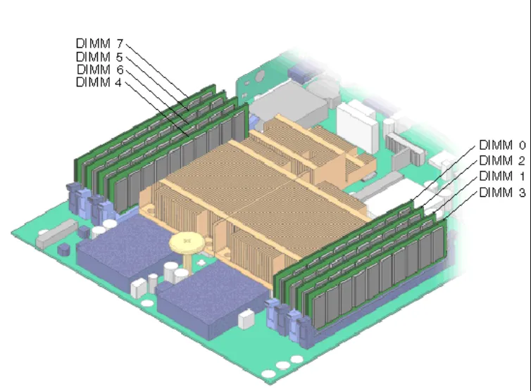
Special consideration: For DIMM or PCI sockets, include the "ear" or latch that protrudes when a card is installed. Maintain a net 2 mm keep-out to the BGA envelope.
Why These Rules Matter
1. Bottom-Side Restriction: Prevent Damage and Enable Controlled Rework
A BGA rework station uses localized heating: a top-side hot-air nozzle focuses heat on the package while a bottom-side preheater elevates the PCB temperature to reduce thermal gradients and shorten time to reflow. When the solder reaches the lead-free melting point around 217 °C, heat readily conducts through the board thickness into the bottom-side component bodies and solder joints.
-
Heat conduction and thermal mass: Large components directly beneath the BGA significantly affect local heat flow. Their bodies and terminations act as thermal masses and heat sinks that pull energy away from the BGA joints, forcing longer dwell times and higher nozzle temperatures to achieve reflow at the BGA interface. At the same time, those large parts absorb heat and are exposed to prolonged elevated temperatures.
-
Obstruction and shadowing: Tall or bulky bottom-side parts under the BGA footprint can physically limit how closely the board can be brought to the preheater or how uniformly heat can be applied across the footprint area. This creates hot and cold spots that make joint temperature control more difficult and inconsistent.
-
Failure modes when large parts are present under the BGA:
- Plastic body softening or cracking; scorched PCB surfaces due to excessive dwell or overheated areas.
- Electrolytic capacitor venting; internal electrolyte can boil and vent under rework temperatures, effectively a "micro-explosion."
- Unintentional bottom-side reflow; solder joints on the underside parts may re-melt, causing components to tilt, shift, or fall off.
Confining the bottom-side keep-out zone to 3216 (imperial)/3225 (metric) and larger components avoids these risks. Small passives such as 0402/0603/0805 present much less thermal mass and are less likely to obstruct heat flow or suffer damage at the bottom-side preheat temperature. This simple rule greatly increases the probability of successful, repeatable rework without collateral damage.
2. Same-Side Clearance: Room for Nozzles, Airflow, and Vacuum Pick-Up
Successful BGA rework also depends on physical access and controlled airflow. The hot-air nozzle must seal reasonably well around the BGA perimeter to establish a stable heat zone, and the vacuum pen or pick-up tool needs clearance above the component to lift it cleanly after reflow.
-
Why 2 mm and 4 mm matter: These spacings minimize the risk of collision between the rework fixtures (clamps, nozzles, nozzles' skirts) and neighboring components. They also allow airflow to circulate around the nozzle without being deflected by adjacent tall parts, which would otherwise create thermal shadowing and uneven heating across the BGA.
-
DIP through-hole parts need extra space: Through-hole leads and barrels are susceptible to heat damage and loosening if exposed to high rework temperatures and forced air. A 4 mm spacing reduces the chance that hot air impinges on the DIP pins or that mechanical fixtures rub against them. It also helps keep the thermal profile for the BGA isolated from wave-soldered joints in the immediate vicinity.
-
Connectors and latches: Large SMT connectors—especially DIMM and PCI slots—often have latch "ears" or card retainers that protrude into the BGA's vicinity when assembled. Treat the assembled envelope as the reference and maintain the 2 mm keep-out to avoid mechanical interference and thermal damage during rework.
How to Apply These DFM Rules in Practice
To ensure your design passes DFM review and remains serviceable in the field, verify the following before release:
1. Identify High-Risk Components
In your layout and Gerber review, mark components that are likely candidates for hot-air rework or that can obstruct rework access:
- BGA packages (including CPU sockets).
- QFN/LGA packages, especially those with large exposed pads or very fine-pitch pins.
- SMT connectors longer than 25 mm (for example, memory sockets and power connectors).
2. Verify the Bottom-Side Keep-Out Zone
- Open the CAM data (e.g., in CAM350) and project the BGA body outline onto the bottom layer to create a clear "under-BGA" zone.
- Within this zone, prohibit any component larger than 3216 (imperial)/3225 (metric). Allow only small chip resistors and capacitors within the footprint projection.
- Where practical, formalize this as a placement keep-out on a mechanical or assembly layer so the rule is enforced by DRC throughout layout.
3. Check Same-Side Spacing Around the BGA
- Measurement tool: Use the CAD tool's measurement function to check clearances.
- What to measure: From the BGA body edge to the nearest neighboring component body edge or pad edge—whichever is closer.
- Enforce the spacings:
- To DIP through-hole components: ≥ 4 mm.
- To tall parts/connectors: ≥ 2 mm.
- To standard low-profile passives: ≥ 1 mm.
- Account for assembled envelopes: For connectors with latches or removable cards, measure against the installed hardware outline, not just the base footprint.
- Document in fabrication/assembly notes: Add rework keep-outs and clearance notes to the assembly drawings to align expectations with the manufacturing team.
Summary
These DFM rules are not arbitrary numbers; they originate from extensive rework experience and failure analysis. BGA rework success depends on two things: adequate physical space for controlled, uniform heating and a thermal profile that does not overexpose neighboring parts. Denying space forces higher temperatures and longer dwell times, multiplying the risk of damage and rework failure.
Give BGAs room to "breathe," both under the footprint and around the body. Keeping components larger than 3216 off the bottom-side projection and maintaining 1/2/4 mm same-side spacing substantially improves yield, reduces repair cost and time, and protects surrounding components from thermal and mechanical stress during rework.
In short, BGA rework success rate = sufficient clearance + appropriate temperature profile.