Practical ESD Protection Methods for Reliable Electronic Device Design
Electromagnetic compatibility (EMC) is a core requirement in modern electronic product design. Among the many EMC threats that hardware teams must manage, electrostatic discharge (ESD) is one of the most frequent and one of the most damaging. An ESD event can inject a fast, high-voltage transient into a circuit through a connector, enclosure gap, cable, or even a nearby operator. If that energy reaches a sensitive pin, the result can be an immediate functional failure, a latent defect that appears later in the field, or a permanent device failure.
Effective ESD protection is rarely the result of a single component. It is the combined outcome of a controlled grounding system, properly selected suppression devices, electrostatic shielding, disciplined PCB layout, and targeted protection at exposed interfaces. The methods below summarize a practical engineering approach that reduces ESD-related failures and improves long-term product reliability.

Design a Proper Grounding System
A robust grounding system is the first line of defense against ESD. When an electrostatic discharge strikes an enclosure, cable shield, or connector shell, the resulting charge must have a low-impedance path to a defined reference. If that path is missing, interrupted, or poorly bonded, the transient voltage rises at the point of entry and couples into nearby traces, ICs, and analog nodes.
Connecting metal enclosures, connector shells, heat sinks, and other conductive structures to a single reference point helps disperse and absorb ESD-induced charge. The objective is not merely to "have a ground," but to establish a consistent return path so that discharge current does not seek unintended routes through signal traces or power planes. A well-designed ground reduces the voltage that appears across sensitive components and lowers the risk of irreversible damage during an ESD event.
In practice, this means paying attention to bond integrity as well as topology. High-impedance joints, painted surfaces that prevent metal-to-metal contact, long ground straps, and fragmented ground islands all increase the local voltage developed by a fast transient. A continuous, low-impedance ground structure gives the discharge a predictable path and keeps more of the event energy outside the sensitive circuitry.
Use ESD Suppressors
ESD suppressors are passive protection devices designed to absorb and clamp overvoltage during an ESD event. They remain high impedance under normal operating conditions and become conductive when the voltage on a protected line exceeds their clamping threshold. Once they conduct, they divert ESD energy to ground and limit the voltage seen by downstream circuitry.
These devices are typically placed on input and output lines, where external cables, user-accessible connectors, and exposed pads create the most likely entry points. Common options include protection diodes, transient-voltage-suppression (TVS) diodes, and metal oxide varistors (MOVs). Each of these devices can respond quickly enough to conduct ESD energy away from sensitive nodes, but they are not interchangeable in every application. The correct choice depends on the line voltage, the expected stress at that interface, board space, and the amount of capacitance the circuit can tolerate.
Placement is as important as device type. A suppressor that is electrically far from the entry point leaves a length of unprotected trace between the connector and the clamp. That trace can still couple energy into adjacent nets before the suppressor turns on. Locating the device close to the interface, with a short, low-inductance path to the local ground, allows the clamp to act before the transient has traveled deep into the board.
Apply Electrostatic Shielding Materials
Shielding materials in the device enclosure help mitigate ESD effects by interrupting the coupling path between an external discharge and internal circuitry. Conductive foils, static-shielding films, and conductive coatings can encapsulate or cover electronic assemblies so that electrostatic fields and discharge currents remain on the outer surface rather than reaching sensitive nodes.
Applying shielding to enclosures and critical circuits reduces ESD coupling into analog front ends, high-impedance sensor inputs, radio sections, and other vulnerable blocks. Shielding is most effective when it is electrically continuous and bonded to the grounding system. A shield that is floating, interrupted by large slots, or connected through a high-impedance path can itself become a coupling structure instead of a barrier.
Shielding does not replace suppression devices. It reduces the amount of energy that reaches internal nets, while suppressors clamp the energy that still arrives at exposed lines. Used together, the two methods address both radiated or coupled ESD energy and conducted transients on connectors and cables.
PCB Layout and Design Considerations
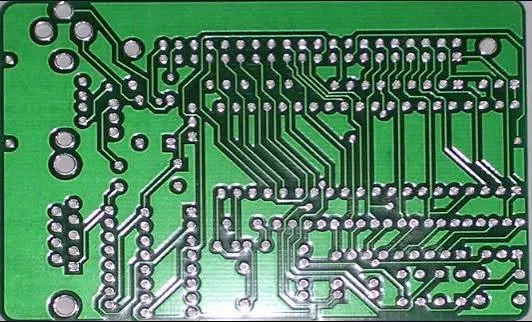
PCB layout and circuit design have a direct influence on ESD susceptibility. An ESD pulse is a fast transient. Any abrupt impedance change, long high-impedance path, or poorly referenced return can convert that pulse into ringing, overshoot, and coupled noise that stresses components far from the original strike point.
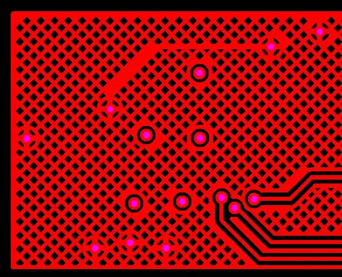
Avoiding abrupt impedance discontinuities and long, high-impedance routes reduces the impact of ESD transients on nearby devices. Short, controlled paths at connector entries, continuous reference planes, and careful grouping of unprotected versus protected nets all help contain the event. Ground pours and well-defined shielding structures on the board can further limit how far an ESD current spreads before it is returned to the enclosure or system ground.
Filters also play a useful role. A filter placed near an exposed interface can attenuate high-frequency content associated with the ESD edge, reducing the energy that continues into the inner circuit. The filter must be referenced to the same local ground used by the suppressor; otherwise the return path becomes part of the coupling loop. Layout details such as via placement, stitch vias around shield cans, and the separation between dirty connector grounds and quiet analog grounds determine whether these structures actually contain the transient or simply relocate it.
Board-level design should also consider secondary effects. An ESD current that is successfully diverted to ground can still produce a ground bounce if the return path is inductive. That bounce can couple into other circuits sharing the same reference. Keeping the high-current ESD return short and local, then connecting that local ground to the broader system reference with a controlled bond, reduces this secondary disturbance.
Add Targeted ESD Protection at Exposed Interfaces
Dedicated ESD protection devices should be placed at critical circuit nodes rather than only at a few generic locations. I/O ports, antenna connectors, user buttons, USB and other cable interfaces, and any pad that a person or cable can touch are typical entry points. ESD diodes or TVS diodes at these locations provide focused protection and are effective at preventing ESD-induced malfunctions at vulnerable interfaces.
Targeted protection works because it intercepts the transient at the boundary of the product. Once the pulse has traveled across a long trace, through a connector pin, and into an IC bond wire, the opportunity to clamp it cleanly is reduced. Protection at the connector or antenna feed keeps the clamp physically and electrically close to the threat and leaves the inner circuit operating closer to its intended voltage range.
The same principle applies to unused or secondary interfaces. An unused connector is still an ESD entry point if it is accessible. Leaving those pins unprotected, or routing them as long stubs, can create unexpected coupling paths. Treating every exposed conductor as a potential ESD node keeps the protection strategy consistent across the product.
Building a Combined ESD Protection Strategy
None of these methods is sufficient in isolation. A grounding system without clamps can still allow a large voltage to appear at an I/O pin. Suppressors without a low-impedance ground cannot divert energy effectively. Shielding without bonded enclosure grounds can leave gaps that couple energy inward. Careful PCB layout without interface protection still leaves the most likely strike points exposed.
A practical design therefore layers the methods. The enclosure and connector shells are bonded into a defined ground reference. Suppressors and, where appropriate, filters are placed at exposed lines with short returns to that reference. Shielding materials and board-level ground structures reduce coupling into internal circuits. Layout rules keep high-impedance and sensitive nets away from ESD current paths. Targeted devices protect the remaining entry points that users and cables can reach.
As electronic devices become smaller and more highly integrated, the physical distance between an ESD entry point and a sensitive node continues to shrink. That makes grounding quality, suppressor placement, shielding continuity, and PCB return-path control more important, not less. Combining a proper grounding system, ESD suppressors, shielding materials, disciplined PCB layout, and targeted protection components reduces the impact of ESD on the product and improves overall robustness in both design verification and field use.