This article uses clear current-path illustrations to explain how a single-phase bridge rectifier works, why its output is a full-wave waveform, and what that implies for the DC output level and component selection. While the topology is simple, understanding the conduction sequence and the resulting voltage and current characteristics is essential for reliable power design and PCB implementation.
How a Bridge Rectifier Works
A bridge rectifier uses four diodes arranged so that, regardless of the polarity of the AC input, current through the load always flows in the same direction. Two diodes conduct during each half-cycle: one connects the higher-potential side of the AC source to the positive output, and another returns the lower-potential side of the source to the negative output (ground). The other two diodes block, isolating the load from reverse voltages.
Positive Half-Cycle: Current Path
During the positive half-cycle of the AC input (when the transformer secondary’s upper terminal is more positive than the lower terminal), current flows from the higher-potential secondary terminal through the first conducting diode into the positive output node, passes through the load, and returns via the second conducting diode to the lower-potential secondary terminal. The remaining two diodes are reverse-biased and do not conduct.
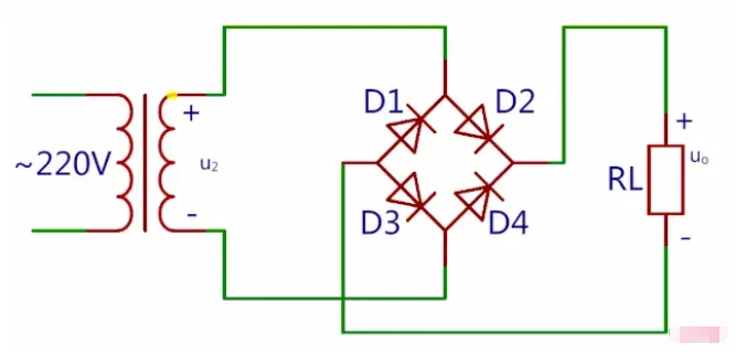
Figure 1 | Current path during the positive half-cycle at the transformer secondary
Negative Half-Cycle: Current Path
When the AC polarity reverses (the previously lower terminal becomes more positive), the conducting pair of diodes swaps. The new pair routes current from the now-positive secondary terminal to the positive output node, through the load, and back to the now-negative secondary terminal. Again, two diodes conduct in series, and the other two remain reverse-biased. Critically, the load still sees the same current direction as in the positive half-cycle, which is why the output is a rectified, unipolar waveform.
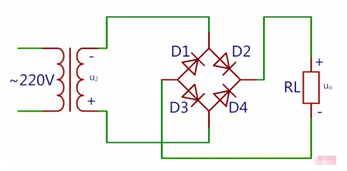
Figure 2 | Current path during the negative half-cycle at the transformer secondary
Full Cycle: Continuous Unipolar Load Current
Over a full AC cycle, conduction alternates between the two diode pairs. The load always sees current flowing into its positive terminal and returning from its negative terminal, producing a full-wave rectified output. The ripple frequency at the output is twice the line frequency because both halves of the sine wave contribute to the output.
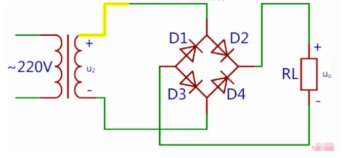
Figure 3 | Current path over a full AC cycle
Output Waveform and DC Level
The bridge rectifier’s output waveform is the absolute value of the input sine wave: a full-wave rectified sine. For an ideal rectifier with no filter and negligible diode drops, the average (DC) value of a full-wave rectified sine is approximately 0.9 times the RMS value of the AC input across the rectifier. This follows from the relationship that the average of a full-wave rectified sine is 2/π times the peak value, and the RMS-to-peak relationship for a sine wave is √2. Multiplying those factors gives approximately 0.9.
In practice, the actual DC output depends on load and diode characteristics. Because two diodes conduct in series in each half-cycle, the DC level is reduced by roughly twice the forward drop. At low voltages or high currents, these forward drops and their temperature dependence become significant design considerations. When a smoothing capacitor is added, the output becomes a quasi-DC voltage that charges near the peak of the rectified waveform and discharges between peaks. The no-load DC output tends toward the peak of the AC waveform minus two diode drops, and under load the ripple and the average level depend on the load current and the size of the filter capacitor.
Key Practical Notes for Bridge Rectifier Design
The following engineering points help translate the operating principle into reliable hardware:
- Diode wiring and orientation: A bridge consists of four diodes arranged so two anodes meet at the negative output, two cathodes meet at the positive output, and the remaining anode and cathode of each pair connect to the two AC terminals. Miswiring a single diode can short the AC source or reverse-bias the load, so verify the polarity markings and PCB silkscreen against the schematic symbol before soldering.
- No center tap required: Unlike a full-wave rectifier using a center-tapped transformer, the bridge uses a two-wire secondary without a center tap. This simplifies transformer selection and can improve transformer utilization, but it introduces two series diode drops during conduction.
- Two diodes conduct per half-cycle: In each half cycle, two diodes conduct in series, and the other two are reverse-biased. The conduction path includes two forward drops, which lower the available DC output and dissipate power as heat. Select diodes with appropriate forward characteristics for the expected current and ambient temperature.
- Full-wave output and ripple frequency: The bridge produces a full-wave rectified output, so the ripple frequency is twice the line frequency (2f). For a given load current and filter capacitor, the ripple magnitude is lower than with half-wave rectification because the time between peaks is halved.
- Average DC level: For an ideal full-wave rectifier without filtering, the DC output is approximately 0.9 times the RMS value of the AC input at the rectifier. Real circuits depart from this due to two forward drops, transformer regulation, and load effects. With a reservoir capacitor, the no-load output approaches the AC peak minus two forward drops; under load, the average DC is lower and ripple increases as load current rises or capacitance decreases.
- Diode voltage and current ratings: Each diode in a bridge must withstand the peak inverse voltage (PIV) imposed across it when it is reverse-biased. In a bridge, the required PIV is approximately the peak of the transformer secondary voltage. Ensure the selected diodes’ repetitive peak reverse voltage rating exceeds this with margin. Current rating must cover the rectifier’s RMS current and allow for surge currents, especially when charging large capacitors at power-on.
- Forward drop and efficiency: The double forward drop in a bridge makes the rectifier less efficient than a center-tapped full-wave rectifier at low output voltages. For low-voltage, high-current supplies, Schottky diodes can reduce forward drop and switching losses. At higher voltages or temperatures, use diodes rated for the thermal and electrical conditions, and verify junction temperature with thermal models or measurement.
- Filter capacitor and ripple: In capacitor-input filters, the ripple magnitude is approximately the load current divided by the product of the ripple frequency and the capacitance. Increasing capacitance or ripple frequency reduces ripple. However, larger capacitors increase inrush current at power-on, so consider surge limiting or NTC thermistors when appropriate.
- Transformer and wiring considerations: The bridge draws high current pulses near the peak of each half-cycle when charging a reservoir capacitor. This increases transformer copper and core losses compared to a purely resistive load. Choose a transformer with adequate VA rating and regulation, and keep the AC loop area small on the PCB to minimize electromagnetic interference.
- Thermal management: The power dissipation in the bridge equals the average load current times the total forward drop (approximately two diode drops). Provide sufficient copper area, heat sinking, or airflow to maintain junction temperatures within limits. For packaged bridge modules, follow the manufacturer’s mounting and heat dissipation guidelines.
- Testing and verification: After assembly, verify that the load sees a unipolar voltage and that the positive and negative outputs are correct with respect to the AC input terminals. Measure the no-load and loaded DC output levels and ripple to confirm they match calculations and expectations.
Summary
- Pay careful attention to the four-diode connection and polarity when drawing schematics and laying out the PCB.
- A bridge rectifier uses a two-wire transformer secondary and does not require a center tap.
- In each half-cycle, two diodes conduct in series while the other two are reverse-biased.
- The output is a full-wave rectified waveform; in the ideal unfiltered case, the DC output is about 0.9 times the pre-rectification RMS value. Real designs must account for diode forward drops, load, and filtering.
With a clear understanding of the conduction paths and waveforms, you can select components and design the PCB to achieve the desired DC output, control ripple, and ensure safe thermal operation in bridge-rectified power supplies.