Most high-voltage FR4 layouts I review do not fail because someone forgot IPC-2221. They fail because one CAD spacing rule was used for two different physical problems. Treat creepage and clearance as the same gap and the board usually passes a dry hipot. It does not stay healthy after flux, dust, and a few hundred hours at working voltage.
The starting mistake is consistent. The constraint table gets a single "HV spacing" value — copied from IPC-2221 or from a 48 V board — and that number is applied to every net above a few tens of volts. Compact placement wins the review. Isolation is assumed to have been handled.
It was not. Split FR4 PCB creepage vs clearance before the plane pours go down.
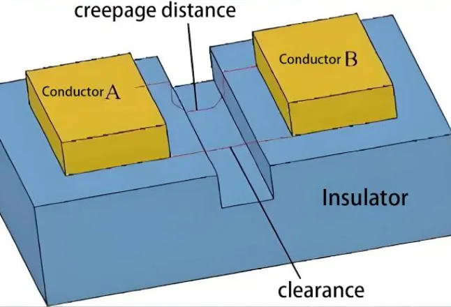
Clearance Is Through Air. Creepage Is the Path Along FR4.
Clearance is the shortest distance through air between two conductive parts. Flashover. Impulse. A solder ball on a pad. A heatsink that was never in the Gerber.
Creepage is the shortest distance along the insulation surface. On a PCB that surface is mask over FR4, bare laminate in a mask opening, the board edge, the wall of a routed slot, or the path around a component body. Tracking lives here. So do humidity films and ionic residue.
Air breakdown is fast. Surface tracking is slow. A board can sit on a hipot fixture at 1500 VAC for one second and still carbonize a path months later between a PFC node and a grounded mounting hole.
CAD does not know the difference. A keepout is a keepout. Constrain only copper-to-copper and you constrained clearance. Creepage still has to be measured on the finished surface — mask openings, slots, and outline included.
Why the Voltage Class You Quoted Usually Understates the Gap
IPC-2221 Table 6-1 is a functional spacing table. Not a safety isolation standard. Designers grab B3 because the board has mask, then run 250–400 V working on 0.25–0.50 mm copper spacing.
That is the usual miss. Solder mask is not qualified solid insulation for a safety barrier. Pinholes. Thin corners. Flux in the openings. B3 is a functional coating column. If the product standard is IEC 62368-1, IEC 60664-1, UL 840, or a drive / inverter spec, those documents own the isolation distance. IPC-2221 does not override them.
Clearance scales with peak / impulse and overvoltage category. Creepage scales with RMS working voltage, pollution degree, and material group. Same 400 V DC bus. Two answers. Clearance might land near 3–4 mm at sea level for a typical CAT II impulse. Creepage on standard FR4 in pollution degree 2 is already larger. PD3 jumps again.
Altitude is the other one that drops out of the notes. Clearance derates above 2000 m — roughly 1.5× air gap at 4000–5000 m. Creepage along the laminate does not. One shared constraint is how that derating disappears.
PCB clearance high voltage is not a single CAD rule
If the class is named "HV" and holds one value, it is wrong for at least one net in that class. Functional 48 V, functional 400 V, and a safety-isolated secondary do not share spacing. Inner-layer dielectric thickness is a third number — through-insulation distance, not creepage.
A 0.10 mm prepreg between primary and secondary is not "enough mils." Hipot might pass. Partial discharge is a different conversation. Burying the same nets on a thin core does not fix surface creepage. It changes the failure mode.
CTI Puts Standard FR4 in the Material Group That Costs Millimeters
Comparative Tracking Index sets the IEC 60664-1 material group. Group I is CTI ≥ 600. Group II is 400–600. Group IIIa is 175–400. Group IIIb is 100–175.
Off-the-shelf FR4 sits around CTI 175–250. That is IIIa unless the laminate note says otherwise. High-CTI FR4 (CTI 600) exists. It is not what you get from a stackup that only says "FR-4, Tg 150." Creepage tables punish IIIa. At a few hundred volts RMS, Group I versus IIIa is not a rounding error. CAM will not flag it. If CTI was never specified, you designed creepage for a material you do not have.
Pollution Degree Is the Variable Layout Treats as Optional
PD1 is sealed and clean. Almost nobody building an open FR4 assembly is in PD1. PD2 is indoor, non-conductive dust, occasional condensation. PD3 is industrial — conductive dust, or dry dust that becomes conductive with moisture. Drive cabinet, vented enclosure: PD2 is optimistic.
Creepage grows with pollution degree. Clearance barely notices until condensation bridges the air gap. That is why a layout that "meets PCB clearance high voltage" still tracks along the mask.
Assembly residue is pollution you installed yourself. Flux, wash leftovers in mask wells, solder balls in the isolation zone. Treat the belt as a keepout for parts, vias, silk, and testpoints. Not just copper. Conformal coat buys a lower pollution degree only if it is specified, inspected, and actually covers the barrier. Do not shrink creepage in CAD because "we will coat it."
What Breaks When the Two Distances Are Collapsed
Surface tracking first. A carbon path along the laminate. Permanent. Hipot after that event is theater.
Then the hardware that was not in copper: a clip, a stand-off, an extruded heatsink, a screw head closer than any pad ever was. Clearance is three-dimensional. Gerber-only review misses it.
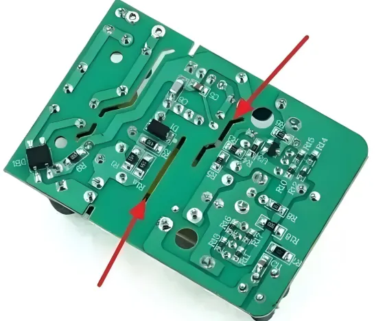
Board edge is a favorite. Copper pulled 0.3–0.4 mm off the outline for fab annular rules, then creepage runs around the edge to a chassis or mounting slot. Edge plating and plated slots make that path conductive. If the slot is the isolation barrier, it cannot be plated and it cannot be 0.4 mm wide. Mechanical routing wants about 1.0–1.5 mm. The electrical path has to go around the ends.
Vias along the barrier look harmless until the mask dam is too narrow and the surface path stitches pad to pad. Same problem when a ground pour fills the unused area next to a boost node.
Layout Rules That Keep Creepage and Clearance as Separate Constraints
Split the constraint system. One class for functional PCB clearance high voltage. A second class for safety creepage. Name them so the next engineer cannot merge them.
Put working voltage, overvoltage category, pollution degree, and material group on the drawing. If the creepage you drew only works on CTI 600 laminate, that CTI is a stackup note, not a hope.
Measure creepage on the assembled surface. Mask openings around HV pads lengthen the conductor. They do not lengthen the insulation. When the board cannot grow, cut an unplated slot. Wide enough to route. Long enough that the path around the ends still meets creepage. Keep clips and cores out of the belt. A Y-cap can sit on the barrier. A random 0603 cannot.
Round the HV copper. Sharp plane edges raise local field at a gap that otherwise "meets the table." Do not use solder mask as the isolation strategy. Check altitude before the outline locks. Clearance moves. Creepage does not. That is the point of treating FR4 PCB creepage vs clearance as two rules.
What to Fix Before the Next Layout Review
If the only HV rule in the CAD file is one millimeter value copied from IPC-2221 B3, the file is not ready. Recalculate clearance from impulse and altitude. Recalculate creepage from RMS voltage, pollution degree, and the CTI you will actually buy. Then walk the assembled 3D path, including the outline.
The board that looks tight and clean in copper is usually the one that tracks. Give the surface a longer walk than the air gap.