










1. Routing Priority
Prioritize critical nets: power, small analog signals, high-speed signals, clocks, and synchronization lines. Follow a density-first approach: begin routing from components with the most complex connections or from the most densely routed board areas.
2. Autorouting
If autorouting produces acceptable quality, it can improve efficiency. Before autorouting, prepare the following:
Autorouter control file (do file): to better control routing quality, define routing rules in detail before running the autorouter. Although many EDA tools provide GUI rule setup, a do file gives more precise control tailored to the design, and the tool runs under the control of that file.
3. Dedicated Layers for Critical Signals
Where possible, allocate dedicated routing layers for clock, high-frequency, and other sensitive signals and minimize their loop area. Use manual priority routing, shielding, and increased clearance when necessary to protect signal integrity.
4. Avoid Sensitive Signals Between Power and Ground Planes
The EMC environment between power and ground planes is often poor. Avoid placing interference-sensitive signals in that region.
5. Place Impedance-Controlled Networks on Controlled Layers
Any network that requires impedance control should be routed on an impedance-controlled layer.
6. General PCB Design Rules
1) Ground Return Loop Rule
Minimize loop area: the loop area formed by a signal and its return should be as small as possible. Smaller loop area reduces emitted radiation and susceptibility to external interference. When splitting ground planes, consider the distribution of important signal routes and avoid problems caused by plane slots. For two-layer boards, fill available areas with reference ground and add vias to connect ground on both sides. Use ground trace isolation for critical nets. For high-frequency designs, pay special attention to ground plane return paths and consider multilayer boards.
2) Crosstalk Control
Crosstalk occurs when long parallel traces on a PCB induce mutual interference due to distributed capacitance and inductance. Countermeasures include:
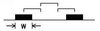
- Increase spacing between parallel traces, following the 3W rule.
- Insert grounded guard traces between parallel signal traces.
- Reduce the distance between the routing layer and the ground plane.
3) Shielding
To minimize loop area, apply shielding for important signals such as clocks and synchronization lines. For very critical or very high-frequency signals, consider coaxial or cable shielding structures: isolate the routed trace on all sides with ground and ensure the shield ground is effectively bonded to the reference plane.
4) Routing Direction Control
Make routing directions orthogonal on adjacent layers to reduce inter-layer crosstalk. Avoid routing different signals in the same direction on adjacent layers. If board constraints make orthogonal routing impossible, especially at high data rates, isolate routing layers with ground planes or use grounded signal traces between layers.
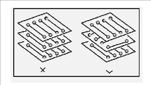
5) Dangling Trace Checks
Avoid floating or open-ended traces (dangling lines) to prevent antenna effects, which can cause unintended emission or reception and unpredictable behavior.
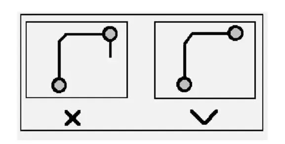
6) Impedance Matching
Keep trace width consistent within the same net. Width changes alter characteristic impedance and can cause reflections at high speeds. When unavoidable, such as at connector or BGA breakout areas, minimize the effective length of inconsistent-width segments.
7) Termination Networks
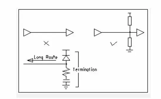
When a PCB trace delay exceeds one quarter of the signal rise or fall time, treat the trace as a transmission line. Match source and load impedances to the transmission line using appropriate termination methods based on topology:
- Point-to-point: use series source termination or parallel end termination. Series is simple and low cost but increases delay. Parallel end termination provides better matching but is more complex and costly.
- Point-to-multipoint: for daisy-chain topologies, prefer end parallel termination. For star topologies, follow point-to-point guidance.
Consider cost, power, and performance; perfect matching is not always necessary—limit reflections to acceptable levels.
8) Loop Closure Rule
Prevent signal traces from forming self-loops across different layers, especially in multilayer designs, as loops increase radiated interference.
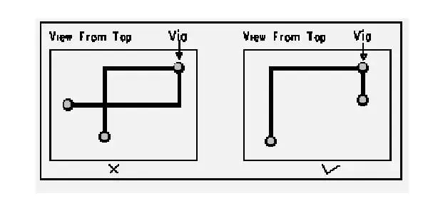
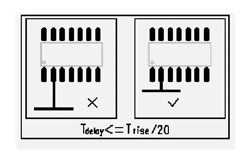
9) Branch Length Control
Control branch stub lengths. A typical requirement is Tdelay <= Trise/20.
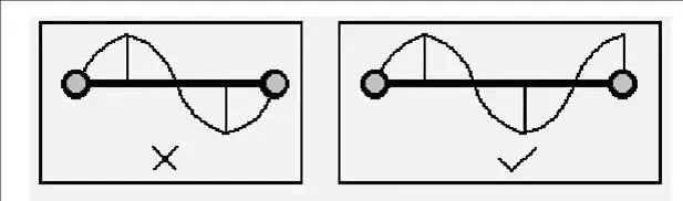
10) Resonance Rule
Avoid trace lengths that are integer multiples of the signal wavelength to prevent resonance for high-frequency signals.
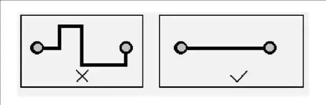
11) Trace Length Control
Keep traces as short as possible to reduce interference, especially for critical nets like clocks. Place oscillators as close as possible to the target device. When driving multiple devices, select network topology according to the specific requirements.
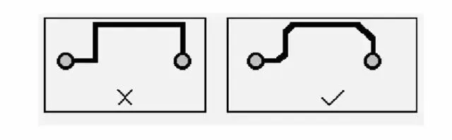
12) Corner Chamfer Rule
Avoid sharp and right-angle corners in routing to reduce unwanted radiation and to improve manufacturability.
13) Component Decoupling
A. Add necessary decoupling capacitors on the PCB to filter power supply noise and stabilize the supply. In multilayer boards the capacitor placement is less critical, but in two-layer designs the layout and power routing directly affect system stability.
B. For two-layer boards, route power through filter capacitors before reaching devices and consider downstream noise. Bus-structured power distribution can help; also account for voltage drop over long traces and add power filter loops when needed to avoid potential differences.
C. In high-speed designs, correct use of decoupling capacitors is essential for board stability.
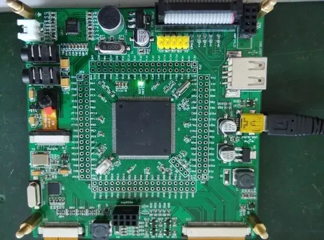
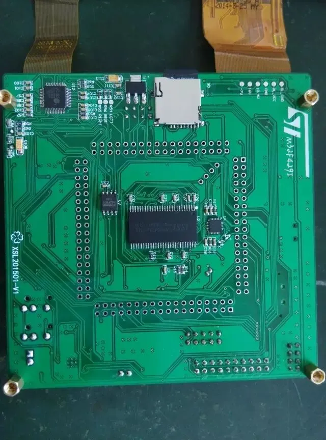
14) Component Placement Partitioning
A. Separate modules of different operating frequencies to prevent mutual interference and shorten high-frequency routing. Place high-frequency sections near interfaces when possible, while considering interference to low-frequency parts. Split ground planes and connect them at a single point at the interface.
B. For mixed-signal designs, place analog and digital circuits on opposite sides of the PCB and use an intermediate ground layer for isolation.
15) Isolated Copper Area Control
Isolated copper areas can cause unpredictable issues. Tie isolated copper to a signal or ground, or remove them. PCB manufacturers often add copper pour on unused board areas to facilitate fabrication and reduce board warp.
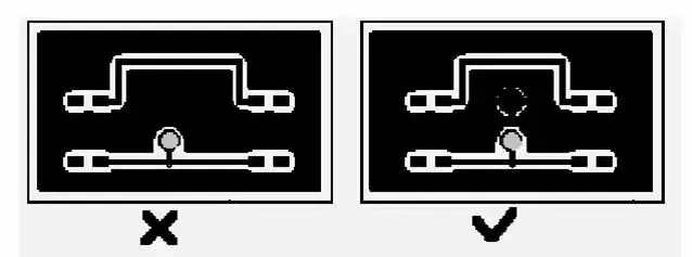
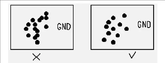
16) Integrity of Power and Ground Layers
In via-dense regions, avoid creating connected cutouts that split the power or ground planes. Plane splitting increases signal return loop area and degrades performance.
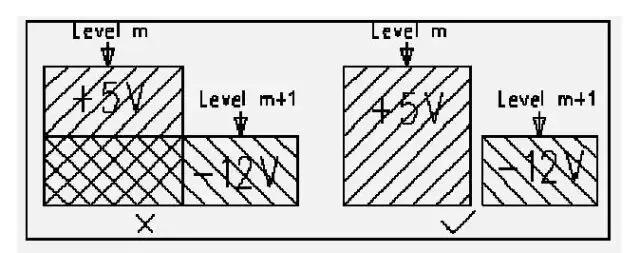
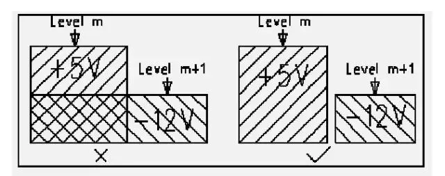
17) Overlapping Power Planes
Avoid overlapping different power planes in the same space to reduce interference, especially when the power rails have significantly different voltages. If overlap is unavoidable, consider an intermediate ground plane.
18) 3W Rule
To reduce crosstalk, ensure adequate spacing between traces. When center-to-center spacing is at least 3 times the trace width, about 70% of the electric field is isolated. To reach about 98% isolation, use 10W spacing.
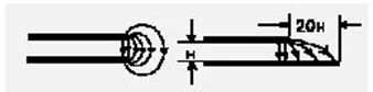
19) 20H Rule
Edge effect: because the field between power and ground planes varies near board edges, some emission occurs at edges. Shrink the power plane inward so the field is confined within the ground plane. H is the dielectric thickness between power and ground. Shrinking by 20H contains about 70% of the field; 100H contains about 98%.
20) The 5-5 Rule
Layer-count guideline: when clock frequency reaches 5 MHz or pulse rise time is less than 5 ns, use a multilayer PCB. If two-layer boards are used for cost reasons, dedicate one side as a continuous ground plane when possible.






