FR4 does not move heat. Copper does. Most thermal problems on an FR4 board start at placement, long before copper weight or via count is discussed. Once a hot package is dropped next to a temperature-sensitive part, or boxed in by keep-outs with no copper path out, later layout tricks only recover a few degrees.
FR4 PCB component placement thermal work is not about spreading parts evenly for a pretty layout. It is about identifying what actually dissipates power, giving those packages a spreading path, and keeping everything else out of the hot zone.
Identifying Heat Sources Before Routing Starts
Start with power, not with package size. A small DFN regulator at 1.5 W is a heat source. A large connector carrying signal current is not. Linear regulators, synchronous bucks, MOSFETs, LED drivers, motor drivers, and processors with high duty-cycle cores are the usual list. Add anything with a θJA number that only works if the copper around it is large.
Datasheet θJA assumes a JEDEC test board, not your four-layer FR4 stackup. Treat that number as a ranking tool, not a prediction. Two parts with similar θJA can run 15–20 °C apart once one sits over a solid ground plane and the other sits over a split plane with no thermal vias.
Mark the heat sources on the floorplan first. Then mark the heat-sensitive parts: crystal oscillators, analog references, electrolytic capacitors, optocouplers with tight CTR, and any sensor whose offset drifts with temperature. Those two lists should not share a neighborhood.
Component Spacing That Lets Heat Leave the Package
Spacing is not just assembly clearance. A 0.5 mm gap between two QFNs may pass DFM and still couple heat through the copper pour that both pads share. If two dissipating parts sit on the same small island, they heat each other. The local copper temperature rises and both junction temperatures follow.
Give high-power packages room for copper, not just room for the pick-and-place nozzle. A DPAK or PowerPAK usually needs several hundred mils of unbroken copper in at least one direction before the next tall part or connector body blocks airflow and spreading. Stacking three bucks in a 15 mm square looks efficient on a placement drawing. On FR4 it creates one hot island that no amount of later via stitching fully cools.
Keep temperature-sensitive parts at least one spreading length away. On a typical 1 oz outer layer that length is often 10–20 mm for a 1 W source before the copper temperature rise becomes small. Closer than that, the analog circuit sits in the thermal gradient whether the schematic shows a connection or not.
Assembly still matters. Tall parts next to a hot package block natural convection. Heat sinks and clips need keep-out that is mechanical, not just electrical. Do not discover that after the board is already routed.
Heat Spreading Paths Run Through Copper, Not FR4
FR4 thermal conductivity is about 0.3 W/m·K through the laminate. Copper is roughly 400 W/m·K. The dielectric is an insulator for heat almost as much as it is for voltage. PCB thermal component placement only works if every hot pad has a continuous copper path to a large plane or pour.
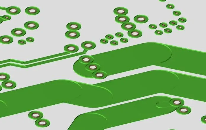
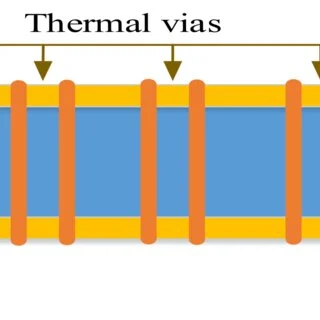
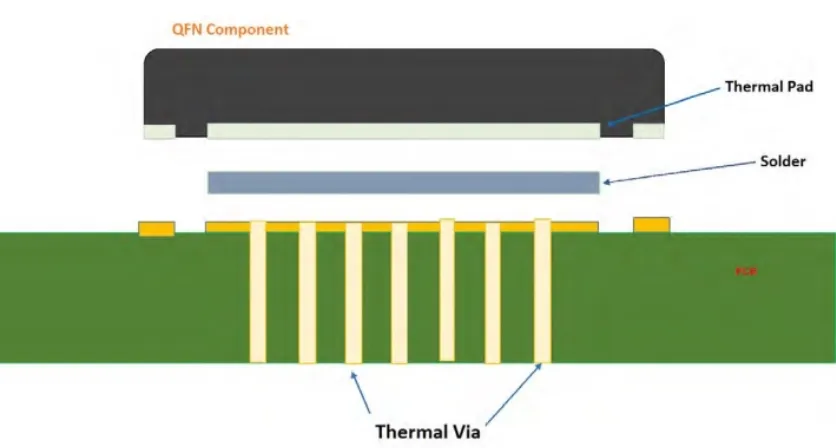
That path is usually: thermal pad or exposed tab → local pour on the component layer → thermal via array → inner ground or power plane → more copper area. Break any step and the temperature rise jumps. A via fence that stops at a split plane is not a path. A pour that necks down to 10 mils between two connectors is not a path.
Place the part so the spreading direction is open. If the only available copper is toward the board edge, put the package so the tab faces that edge. If an inner plane is solid under that region, use it. Do not place a 2 W FET over a plane split that was drawn for return-current reasons and then expect the thermal vias to find another route.
How Much Copper Area High-Power Parts Actually Need
Copper area is the heatsink on most FR4 boards that have no metal housing. Datasheets often show a curve of temperature rise versus copper area for 1 oz and 2 oz. Those curves assume a square pour attached to the thermal pad on a two-layer board in still air. Real boards are better if an inner plane is present, worse if the pour is broken by traces.
For a 1 W surface-mount regulator on 1 oz copper, a few square centimeters of connected copper plus a modest via array is often the difference between 40 °C rise and 80 °C rise. Doubling copper weight helps, but doubling connected area usually helps more at the placement stage because area is still free to choose.
Do not count hatched planes or isolated islands. Count only copper that is electrically and thermally tied to the pad. A ground pour that is 0.2 mm away across solder mask does almost nothing. Thermal vias should be in the pad or immediately adjacent, filled or tented per the fab capability, and tied to the largest plane available.
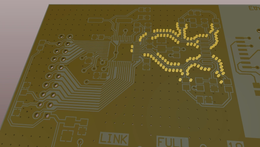
Via count has diminishing returns. The first 9–16 vias under a QFN pad move most of the heat. Adding 40 more vias in a ring far from the pad mainly uses drill capacity. Place vias where the heat enters the board, not where they look symmetric on the courtyard.
Placing High-Power Components Without Creating Hot Islands
High-power layout is a placement problem first. Grouping all power parts in one corner is convenient for a short power tree. It is also how you build a local oven. Separate dissipating packages so each has its own copper field. Share a plane, not a 20 mm × 20 mm pour.
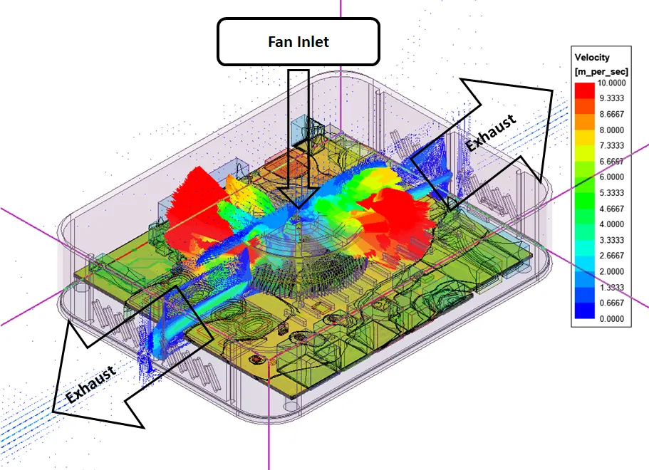
Put the highest dissipation where cooling actually exists. On a board with forced air, that is upstream in the airflow, not behind a tall connector. On a board that conducts into a chassis, that is over the mounting points or the metal standoff region. On a sealed box with only natural convection, spread the sources and keep them off the board center if the center cannot grow copper.
Watch the secondary heat. A buck inductor is not always the hottest part, but the FET and the inductor sit close and the copper between them carries both current and heat. Give that copper width for current and area for heat. Do not route a skinny pour under the inductor footprint and call the thermal design done.
Keep electrolytic capacitors and polymer caps out of the hot copper. Lifetime halves with every 10 °C in many families. That is a placement decision, not a later BOM change.
What Breaks in Fabrication, Assembly, and the Field
Poor thermal placement rarely fails at electrical test. It fails after the product sits at 50 °C ambient with the load applied. Solder joints on large thermal pads can look acceptable and still run the die above the derating limit. Nearby MLCC packages see extra temperature cycling. Analog channels drift. Fans, if present, get asked to fix a layout that never gave copper a chance.
On the fab side, dense via arrays under a pad need a defined drill, plating, and tenting or filling spec. If the vias are open and the paste volume is wrong, solder wicks into the holes and the joint voids. That is an assembly problem caused by a thermal-via decision made at placement time. Call the via treatment before the footprints are locked.
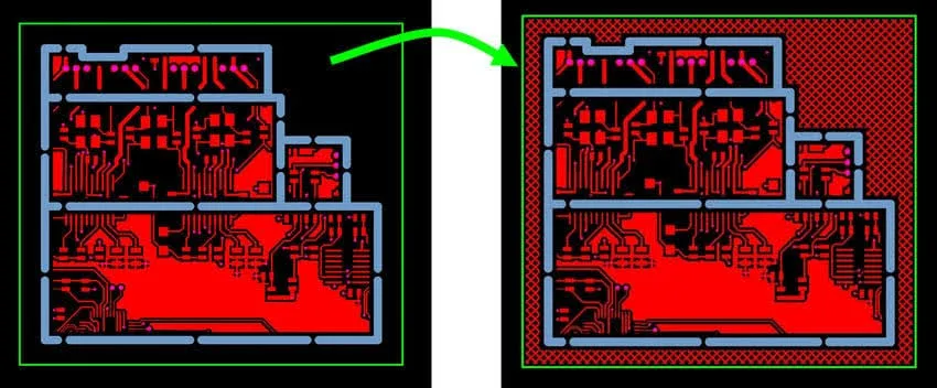
Copper balance still applies. A heavy pour under one corner and an empty region opposite can warp a thin FR4 panel. Spreading the copper for thermal reasons often helps the panel as well, provided the opposite side is not left as isolated scraps.
Placement Rules That Survive a Thermal Review
Identify every real heat source from dissipation, not from package outline. Separate those parts from crystals, references, and lifetime-limited capacitors. Give each dissipating package a continuous copper path into the largest plane you have, and size that copper from the datasheet area curves plus the inner-plane connection you actually routed.
Do not cluster high-power parts onto one island just because the power tree is short. Short electrical path and short thermal path are not the same requirement. FR4 PCB component placement thermal performance is decided when the first high-power courtyard is dropped onto the board. After that, you are only negotiating how many degrees you can still recover.