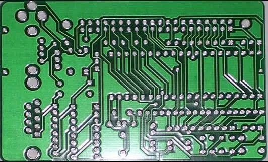
A single FR4 board that places and solders cleanly can still fail in production once it is arrayed. The defect is rarely the circuit. It is the panel: rails too narrow to grip, fiducials the machine cannot see, tooling holes that do not match the fixture, or a V-score that cracks a plane two millimeters inside the outline. FR4 PCB panelization design is a handling and registration problem first. Electrical design comes after the panel can be located and held.
The notes below are the checks that keep showing up when a panel looks finished in CAD and then stops the SMT line.
How the Panel Has to Work as a Mechanical Part
An SMT panel is a temporary workpiece. Conveyors grab the long edges. Pins drop into tooling holes. Cameras look for fiducials. The individual boards only exist after depanel. If any of those three features is missing, undersized, or in the wrong place, the array is not a panel. It is a sheet of FR4 that cannot be processed.
Panel structure therefore starts with the process, not with board count. Ask what the assembler uses: edge-clamp conveyors or pin fixtures, vision on rails or vision on each board, V-score or routed tabs. Then draw the rails, holes, and marks to that process. Filling the panel with as many circuits as possible is the last step, not the first.
A typical production array on 1.6 mm FR4 is two rails on the long sides, global fiducials on those rails, two or three tooling holes, and either a V-score grid or routed tabs with mouse bites. Anything else is a special process and needs a note, not a copied template.

Rail Width That Survives Conveyors and Depanel
Rails exist so the machine never has to grip a finished board edge. They also carry the global fiducials and most of the tooling holes. Width is the first number that gets cut when someone is chasing panel utilization.
5 mm rails work on some lines. They fail on others the first time a clamp or a worn belt catches the copper instead of laminate. 8–10 mm is the range that consistently clears edge clamps, leaves room for a 1 mm fiducial plus keep-out, and still breaks cleanly after assembly.
Do not pour solid copper across the full rail unless there is a reason. A continuous plane on a narrow rail becomes a peel strip during V-score or tab break. Pull copper back from the outer rail edge the same way it is pulled back from a board outline—0.4–0.5 mm is enough. Keep a copper-free zone where the conveyor contacts the laminate.
Rails on only one side look efficient. They twist. Two parallel rails keep the panel flat through reflow. If the array is small enough to run as a single-board panel, the "rail" is still required unless the assembler explicitly accepts board-edge clamping.
Fiducials the Vision System Can Actually Lock
A fiducial is a copper pad the camera uses as a coordinate origin. If solder mask, silkscreen, or a via sits on it, the camera reports a bad mark and the board is skipped or placed blind.
The geometry that works on almost every SMT line:
- 1.0 mm diameter copper pad, circular
- Solder-mask opening 2.0–3.0 mm, centered, no mask on the pad
- No silkscreen inside 3–5 mm of the pad
- No vias, traces, or plane slivers in the mask opening
Global fiducials go on the rails, at least two, preferably three, not in a straight line. Two marks define translation and rotation. The third catches stretch and warp. Place them as far apart as the rail allows. Local fiducials on each board are needed when the individual circuit is fine-pitch or when the panel is large enough that FR4 growth between global marks exceeds the placement tolerance.
Keep fiducials at least 5 mm from the panel outer edge and at least 3 mm from any V-score or route path. A mark that sits on a score line is gone after depanel and is already unreliable before that because the surface is not flat.

Tooling Holes That Match the Fixture, Not the CAD Default
Tooling holes are for pins. Diameter and position have to match the assembler or the fabricator's panel fixture. Copying 3.2 mm holes from the last job is how panels arrive with holes the pins will not enter, or with holes so sloppy the panel walks under the camera.
Common production sizes on FR4 are 2.0 mm, 3.0 mm, and 3.175 mm (1/8 in). Finished hole, not drill. Specify plated or non-plated. Non-plated is usual; plated holes change diameter after plating and can seize on a hardened pin.
Two holes define position. Three holes over-constrain a warped panel and can crack the rail when the third pin is forced. Place the pair on one rail or on opposite corners, far apart, and keep copper and mask away from the hole wall. A 1 mm annular keep-out around a non-plated tooling hole is enough to stop foil from tearing when the pin enters.
Do not put tooling holes inside the finished board unless that board will keep them after depanel. Once the rail is broken off, those holes are gone. If the downstream process needs holes in the product, they are product features, not panel tooling.
V-Score Versus Routed Tabs on FR4
V-score is cheap and fast. It only works on straight lines that run the full panel. The blade leaves a residual web, typically 1/3 of the board thickness. That web is what you snap. It is also a stress concentrator. Planes and traces that cross a V-score line will crack or lift when the panel is broken. Pull copper back from the score centerline the same way it is pulled back from a routed outline—add 0.15–0.20 mm beyond the normal edge rule.
Routed tabs with mouse bites take irregular outlines. They cost more machine time and leave a rougher edge that usually needs a secondary clean-up if appearance matters. Tab width and mouse-bite hole size control break force. Too few tabs and the array folds in reflow. Too many, or tabs that are too wide, and the operator cracks the board while removing it.
Use V-score when the boards are rectangular and the copper can be kept off the score lines. Use routed tabs when the outline is not a straight grid, when components hang near the edge, or when the residual V-score web would violate a thickness or cleanliness requirement.

Mixing both on one panel is common and usually correct: V-score between boards, routed outer profile, tabs only where the array must stay attached to the rail. What is not correct is leaving the choice implicit. The fabricator will pick the cheapest method that matches the outline layer. If that method is wrong for the copper or the components, the first evidence is cracked parts after depanel.
FR4 PCB panelization design is finished when the rails can be clamped, the fiducials can be seen, the tooling holes accept the pins, and the separation method does not tear copper or components. Board count on the panel is a yield number. It is not the design.