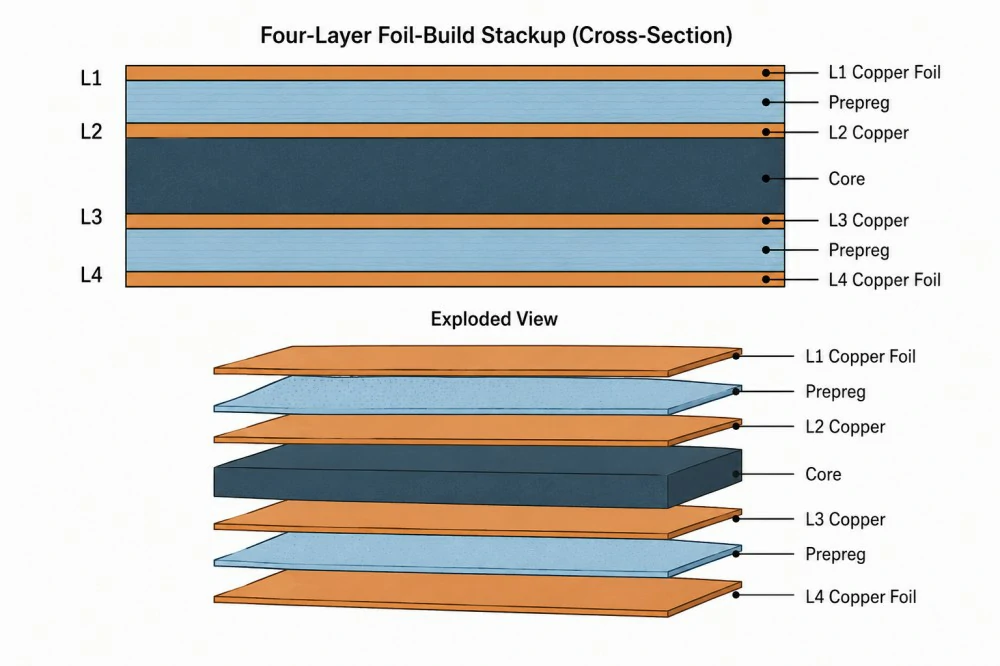
Multilayer pcb layout begins with the stackup, not the first trace. Assign every signal layer a continuous reference plane before you place components. On a typical 6- or 8-layer board that means ground on the layer adjacent to each high-speed signal layer, power planes paired tightly with ground for decoupling, and enough signal layers that the fast edges do not have to hop repeatedly. Once the planes are fixed, the routing either preserves the return path or creates the discontinuities that show up later as eye closure or radiated emissions.
Most layout problems on multilayer boards are return-path problems that look like routing problems until you inspect the planes.
Planning Layers Before Routing Starts
Count the high-speed nets, the power rails, and the density first. A 4-layer board gives two signal layers and one solid ground. Six layers typically add a second ground and one more signal layer. Eight layers give multiple stripline options. Put solid ground next to every signal layer that will carry edges faster than a few hundred picoseconds. Pair at least one power plane tightly with ground so the interplane capacitance helps the PDN. Leave the outer layers for components and short fan-out; put the longest high-speed runs on inner layers where the planes contain the field.
If the pin count forces more layer hops than the stackup can support with nearby stitch vias, add layers before you start routing. Changing the stackup after the layout is frozen is expensive.

Assigning Signals to Layers
Route clocks, differential pairs, and DDR byte lanes on layers that reference solid ground. Outer microstrip works for short connector runs. Inner stripline between grounds reduces crosstalk and radiation for longer runs. Keep matched groups on the same layer so via delay does not create skew. Orthogonal routing directions on adjacent signal layers cut broadside coupling when two signal layers must face each other without a plane between them. Sensitive analog nets stay over continuous ground and away from switching edges; do not split the plane under them unless isolation is mandatory and no high-speed net crosses the gap.
Power and Ground Plane Placement
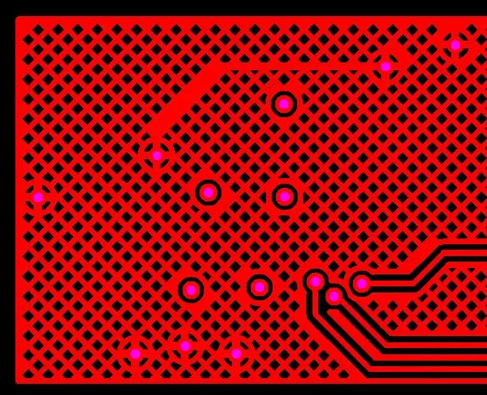
Ground planes should be continuous under every high-speed net. Power planes can be split for multiple rails, but the splits must not sit under critical signals. Place power and ground planes adjacent with thin dielectric between them; the resulting capacitance helps high-frequency decoupling. On multilayer boards the plane pair is usually near the center for mechanical balance and low inductance. Stitch the planes with vias at the board edge and near every high-current switching region. Floating outer-layer pours need the same stitching or they become antennas.

Keeping the Return Path Continuous
Above a few tens of megahertz the return current concentrates directly under the trace on the nearest plane. A continuous ground keeps the loop small and the impedance stable. A split, slot, or dense antipad field forces a detour. The loop area grows, emissions rise, and a reflection appears. On multilayer boards the return can also jump between planes at a layer change. Place a ground stitch via within a few millimeters of every high-speed signal via so the return follows. For differential pairs, place the stitch vias symmetrically. Missing the stitch via is one of the most common findings on multilayer pcb layout reviews.
Via Transitions and Reference Changes
Every via is a discontinuity. On multilayer boards a through-via from an outer layer to an inner layer leaves a stub that can resonate at multi-gigabit rates. Minimize layer changes on the fastest nets. When a via is required, use the same via structure for both members of a differential pair and place the return stitch next to it. Back-drilling removes the unused stub when the data rate makes the length significant. Blind vias eliminate the stub but raise cost. Reference changes from ground to power need a local stitching capacitor or via so the high-frequency return does not spread across the board.

Routing Priority and Crosstalk Control
Route clocks and the tightest differential pairs first. Then DDR byte lanes and other matched groups. Sensitive analog and RF come next. General digital and power last. Spacing starts at 3× trace width center-to-center for moderate edges; clocks and multi-gigabit pairs usually need 5× or more, or they should sit on opposite sides of a ground plane. Parallel length multiplies coupling. Orthogonal routing on adjacent layers reduces broadside coupling. Guard traces only help when stitched to ground at both ends and at intervals; an unstitched guard can increase coupling.
Power Distribution and Decoupling Placement
The power plane and adjacent ground form the low-inductance path for high-frequency current. Place decoupling capacitors close to the pins with short, wide connections and multiple vias so the loop inductance stays below 1 nH. The smallest high-frequency capacitors go nearest the pins. Bulk capacitors sit near the regulators. On multilayer boards the plane capacitance helps above a few hundred megahertz, but it does not replace the local capacitors. Keep high-current switching loops small and away from sensitive analog regions. Stitch the power and ground planes near every high di/dt source.
Post-Layout Checks That Catch Most Problems
After routing, inspect every high-speed net for continuous reference. Confirm no critical trace crosses a split. Check that every layer-change via has a ground stitch within a few millimeters. Verify differential pairs stay together with matched vias and acceptable spacing. Look at decoupling proximity and via geometry. Confirm outer-layer pours are stitched. Run the impedance calculation against the production stackup and review the fabricator's coupon plan. On multilayer pcb layout the planes and the return path set the limit. The routing either preserves that limit or spends it on vias, splits, and long parallel runs. Catch the discontinuities before the board is built.