In electronic product development, PCB design is the hidden foundation. A small routing error can keep a product from passing safety certification, weaken immunity to interference, or cause overheating and burnout. The points below cover safety spacing, EMC practices, placement and routing rules, thermal design, and process details.
Safety Spacing: The First Line of Electrical Safety
Safety spacing is a hard limit in PCB design. It directly affects whether the equipment is exposed to short-circuit and discharge hazards. The two core metrics are electrical clearance and creepage distance.
Key Parameters
- Creepage distance: at 50–250 V input, L–N before the fuse ≥ 2.5 mm; at 250–500 V, ≥ 5.0 mm.
- Electrical clearance: at 50–250 V input, L–N before the fuse ≥ 1.7 mm; at 250–500 V, ≥ 3.0 mm.
- Special requirements: primary to secondary ≥ 6.4 mm (slot the board if spacing at an optocoupler or Y capacitor is insufficient); between transformer windings ≥ 6.4 mm; reinforced insulation requires ≥ 8 mm.
Minimum creepage versus voltage range is shown below.
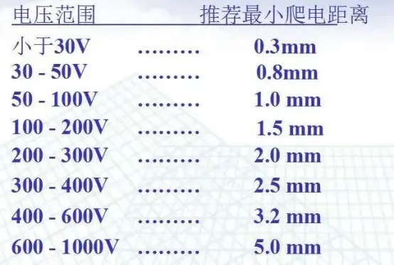
Figure | Voltage range and recommended minimum creepage distance
EMC and Interference Control: Keep the Signal Stable
Electromagnetic compatibility of electronic equipment directly affects how the product behaves in use. Interference-control design is what prevents signal disruption and test failures.
Core Practices
-
Keep traces short and place parts locally
Place the gate-drive resistor next to the MOSFET, place the current-sense resistor next to the IC pin, and keep components around an op-amp close enough to shorten high-impedance traces. That reduces the area that can pick up interference.
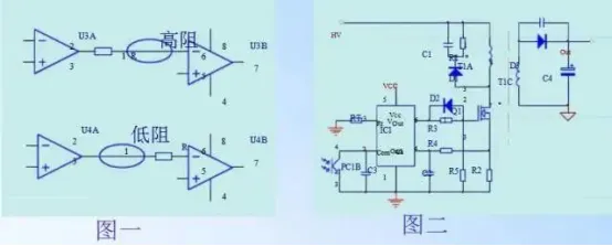
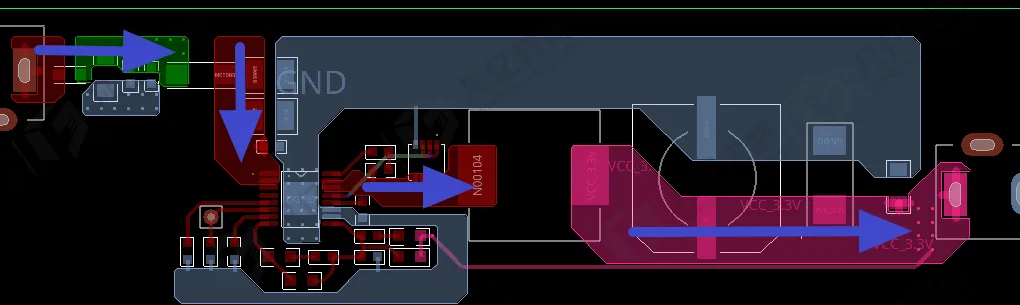
Figure | Layout for long-trace interference control
-
Separate strong and weak signals
Keep small-signal traces at least 2.0 mm from high-current traces. Do not run them in parallel, so they do not couple into each other.
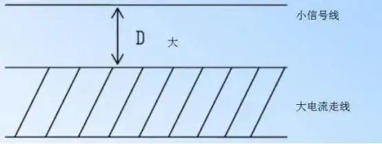
Figure | Spacing between small-signal and high-current traces
-
Ground with intent
When several ICs share a supply, use parallel single-point grounding rather than series grounding, which lets the parts disturb one another. Ground the control loop and the power loop separately. Ground a heat sink at a single point when possible to improve noise rejection.
-
Stay away from aggressors
Keep optocouplers away from high-current traces, transformers, and other strong electric- or magnetic-field parts. Keep MOSFETs and transformers as far as practical from the input terminals so radiated energy does not couple directly into the input and cause an EMI test failure.
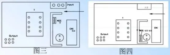
Figure | Effect of MOSFET and transformer placement on EMI
Placement and Routing: Rules That Decide Whether the Board Works
Sound placement and routing improve immunity, simplify assembly, and extend product life.
Board-Level Placement
- Distribute heat sinks evenly and keep the airflow path open. Keep capacitors, ICs, and similar parts away from heat sinks, power resistors, and other heat sources.
- Keep input and output cable lengths consistent, and reserve space for cable ties at connectors. Keep components on the board edge at least 2 mm from the edge.
- Place adjustable parts such as potentiometers and microswitches to match the mechanical design. External adjustment parts must line up with the knobs on the enclosure panel.
Routing Rules
- Match width to current: on 50 μm copper, a 1 mm-wide trace can carry 1 A; on 70 μm copper, it can carry 1.5 A. Make power traces as wide and as short as practical.
- Use smooth corners: avoid right-angle and acute-angle bends. In high-frequency circuits, curved corners are better for electrical performance.
- Keep-out under specific parts: do not run high-voltage traces under inductors, current loops, or metal-film resistors. Do not route signal traces through a transformer or a heat sink.
- Vias: in high-current areas, add vias and add solder to raise current-carrying capacity. On a single-sided board, keep jumpers at a safety distance from low-voltage parts, and at least 1 mm from a heat sink.
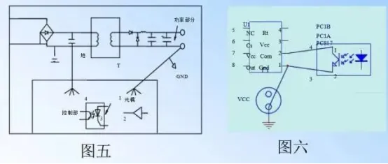
Figure | Single-point grounding of the control loop and power loop
Thermal Design and Process: Stability Together with Manufacturability
Thermal Design
- Keep temperature-sensitive parts such as ICs away from heat sources. Keep small boards at a safe distance from the transformer so semiconductor devices are not damaged by heat.
- Keep heat-generating parts such as power resistors and bridge rectifiers spaced away from capacitors and other parts that age with heat. Where needed, add solder to help conduct heat, without covering pads that must remain open.
Process Details
- Mark the wave-solder direction with an arrow. Orient DIP ICs perpendicular to the wave-solder direction; orient SOP packages the opposite way.
- Provide fiducials for SMT parts (at least two per board, on a diagonal) to improve placement accuracy.
- Size pads correctly: the outer diameter is generally not less than (lead hole diameter + 1.2) mm. On dense digital boards the minimum may be (d + 1.0) mm. Enlarge pads when the hole is larger than 2.5 mm to reduce cold joints.
- When an SMD pin ties into a large copper pour, use thermal relief so concentrated heat during soldering does not damage the part.
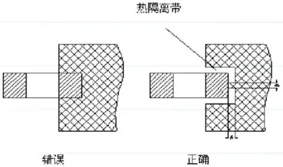
Figure | Thermal relief for SMD devices
Common Failure Cases
-
Placement error
On a six-layer board, a PWM IC and an optocoupler were placed under the MOSFETs, separated by only 2.0 mm of PCB. The resulting interference was severe. Moving them away from the aggressor resolved the problem.
-
Routing error
A current loop enclosed too large an area and picked up excessive interference. The PWM IC sense line ran parallel to the drive line and the two coupled into each other. Shortening the traces and stopping the parallel run restored normal operation.
PCB design is a discipline of details. Safety spacing, EMC, placement, and routing are the controls that reduce design risk and raise product reliability. Use the checklist above as a reference on the next board.