










In day-to-day electronics work, PCB design is a field where a small error can have a large effect. Hundreds of hours of design effort can be wasted by one placement mistake or one overlooked routing choice, leaving the product short of its performance target or unusable.
The points below are grouped into three areas: placement rules, routing details, and fabrication fit. Each item is tied to a working illustration.
Placement Rules: The Foundation of the PCB
Placement is the first step in PCB design and sets much of the later performance. Many interference and debug problems that appear late in a project start as hazards left in the early placement.
1. Keep High Voltage and Low-Level Circuits Physically Apart
On boards such as a switch-mode power-supply high-voltage stage, high-voltage, high-current loops must be completely separated from low-voltage, low-current signal circuits (Figure 1). If the two regions are mixed, electromagnetic interference from the high-voltage loop couples directly into the low-level signals. The result can be false triggering of an IC, corrupted data, and in severe cases a burned circuit.
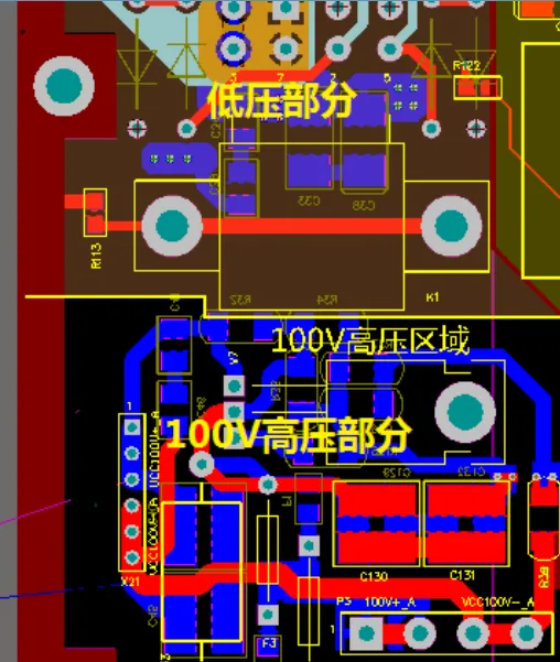
Figure 1 | Isolation of high-voltage loops from low-level signals
2. Place the Crystal Next to the IC to Keep the Clock Accurate
In high-frequency digital circuits, the crystal and oscillator are the timing reference and must sit next to the IC clock pins (Figure 2). Crystal drive strength is limited. If the part is far from the IC, the path picks up external interference and the square-wave frequency at the chip can shift. Without a common clock, the digital system cannot stay synchronized.
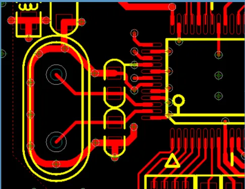
Figure 2 | Crystal placed next to the IC clock pins
3. Use Symmetric Placement for Identical Circuits
When modules are the same and the structure is repeated—for example multiple power rails or identical sensor channels—use a symmetric layout together with the EDA tool's module-reuse function (Figure 3). That reduces repeated drawing time. More important, symmetric placement keeps branch parameters consistent and avoids signal imbalance caused by layout differences. Later debug can then follow the same pattern on every channel.
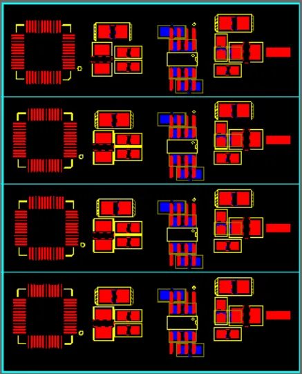
Figure 3 | Symmetric placement with module reuse
4. Leave Room for Debug; Do Not Block Test Points with Large Parts
Plan for later repair and debug during placement. Do not put large components next to small parts. Around test points that a multimeter or oscilloscope probe must reach, such as resistor and capacitor pins, reserve at least 2–3 mm of working space (Figure 4). Cases exist where a large inductor was placed beside a capacitor so a probe could not reach the test point, and the board had to be respun. One extra millimeter in placement can save many steps later.
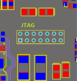
Figure 4 | Clearance around debug and test points
5. Place Decoupling Capacitors Against the IC; Keep the Loop Short
The main job of a decoupling capacitor is to filter high-frequency noise at the IC supply pin. Place it against the IC power pin and keep the loop formed by the capacitor, the supply, and ground as short as possible (Figure 5). If the capacitor is far from the IC, the loop lengthens, filtering drops off, the supply at the IC becomes unstable, and lock-ups or data errors become more likely. The useful distance for a decoupling capacitor is typically no more than 5 mm. Beyond that distance, the capacitor adds little value.
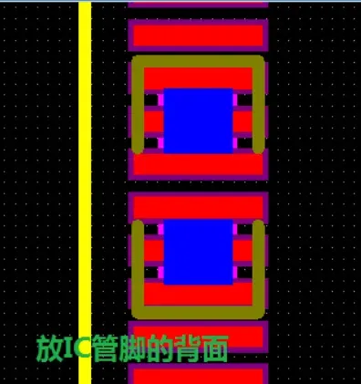
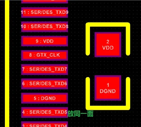
Figure 5 | Short decoupling loop at the IC
Routing Details: Hidden Traps That Destabilize the Signal
Routing is the working path of the design. Even a sound placement fails if the routing is wrong. The five details below are common failure points.
1. Do Not Cross a Split on High-Frequency Signals; Keep the Reference Continuous
Crossing a split means a signal trace leaves one reference plane for another, for example from GND1 to GND2 (upper part of Figure 6). The effect on low-frequency signals is limited, but it must be avoided on high-frequency digital signals such as 100 MHz and above. Crossing a split leaves the signal without a continuous reference, causes an impedance step, and produces severe EMI and crosstalk. After a USB 3.0 pair crosses a split, the rate can fall from 5 Gbps to 1 Gbps, or the link can drop. Keep high-frequency signals over one continuous reference plane (lower part of Figure 6).
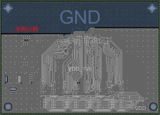
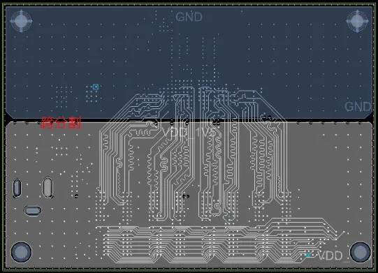
Figure 6 | Crossing a split versus routing over a continuous reference
2. Do Not Exit Chip-Component Pads on a Diagonal; Prevent Rotation
On 0402 and 0603 chip-component pads, a common error is to exit the pads on a diagonal (Figure 7.1). Solder-mask openings can be off by 0.1 mm in fabrication. Diagonal routing then leaves unequal copper exposure on the two sides of the pad. During reflow the solder surface tension is unbalanced and the part can rotate or tilt (Figure 7.2). In severe cases it shorts.
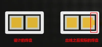
Figure 7.1 | Diagonal pad exit

Figure 7.2 | Rotation and tilt after reflow
The correct method is to fan out symmetrically along the long axis of the pads (Figure 8). If the short-axis routing is also symmetric, placement drift is reduced and yield can rise from 80% to 99%.
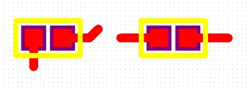
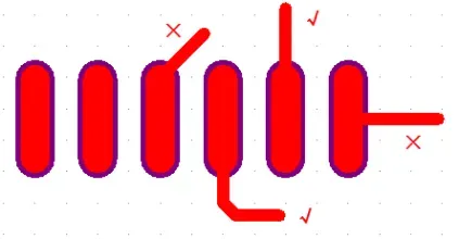
Figure 8 | Symmetric fanout along the pad long axis
Pads of adjacent different nets must not be tied by a direct trace between them (Figure 9). Route to each pad first, then continue the trace. A direct tie between pads lets solder bridge during hand soldering and causes a short. The correct sequence is pad first, then the outgoing trace.
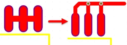
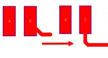
Figure 9 | Adjacent pads of different nets
3. On Differential Pairs, Match Length First; Spacing Can Flex
The value of a differential pair such as HDMI or DDR4 is interference rejection and tight timing, but only if the two traces in the pair are length-matched (Figure 10). Many designers treat equal spacing as more important than equal length. That is not the case. A length mismatch creates delay skew, misaligns the edges, and weakens common-mode rejection. Practical rules:
- Match length first. Keep the error within 10% of the signal period. For a 1 GHz signal, that means ≤ 10 ps, corresponding to a length difference of ≤ 3 mm.
- If length must be added, use small serpentines with a bend radius ≥ 3 times the trace width. Avoid right angles and acute angles.
- Spacing can be adjusted to fit the available area, provided adjacent traces do not create crosstalk.
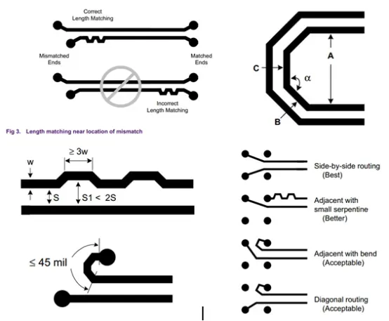
Figure 10 | Intra-pair length matching on a differential pair
4. Guard Clock and High-Frequency Signals with Ground, or Keep 3W Spacing
Clock signals such as a CPU CLK and high-frequency signals such as RF traces are strong aggressors and need shielding:
- If space allows, use ground fencing: run ground beside the signal and place a ground via about every 5 mm (Figure 12) so the interference stays inside the fence.
- If space is tight, keep at least 3W spacing to other signals, where W is the signal width. For a 0.2 mm trace, the spacing is at least 0.6 mm, which reduces coupling into nearby nets.
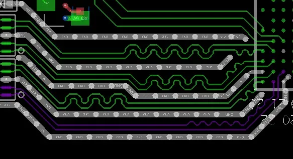
Figure 12 | Ground fencing of a clock or high-frequency trace
5. Do Not Let Vias Slice the Reference Plane; Leave Room for One Trace Between Holes
When placing vias, avoid cutting up the adjacent reference plane (Figure 13). Dense vias in a GND plane can break a continuous ground into fragments, lengthen the return path, raise impedance, and increase interference. Correct practice:
- Space vias far enough apart that at least one signal trace can pass between them. For a 0.2 mm trace width, use spacing ≥ 0.4 mm.
- Place vias toward the edge of the reference plane when possible, so the interior of the plane stays intact.
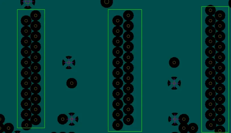
Figure 13 | Vias cutting a reference plane
Fabrication Fit: Design What the Factory Can Build
Many designs focus on electrical performance and ignore whether the board can be produced. The two details below affect both whether the PCB can be built in volume and how long the product lasts.
1. Gold Fingers Must Be Fully Open in Solder Mask; Flaking Mask Will Fail the Contact
Gold fingers, such as those on memory modules and PCIe connectors, are the mating contacts. The gold-finger region must be fully open in the solder mask, with no mask between the pads (Figure 13). If the openings are missed, solder mask covers the gold surface. After repeated insertion and removal the mask flakes, causing poor contact or a short. When building the gold-finger footprint, draw the openings in the solder-mask layer with copper or 2D lines so they are not omitted later.
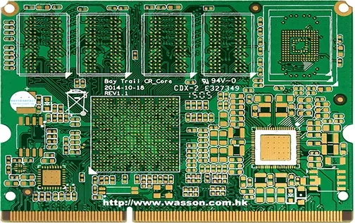
Figure 13 | Full solder-mask opening on gold fingers
2. Keep Footprint Pads Symmetric to Prevent Tombstoning
Tombstoning—one end of a part lifting like a headstone—is common in assembly. The usual cause is an asymmetric footprint (Figure 14). On a 0402 resistor, if the two pads are different sizes, the solder on each side melts at a different rate during reflow. Surface tension pulls the part toward the larger pad and it stands up.
The fix is to keep both pads the same size when the footprint is created (error ≤ 0.1 mm) and to match the pad size to the actual component terminals so solder wets both ends evenly and forms a stable joint.
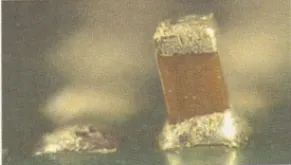
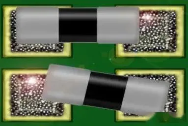
Figure 14 | Asymmetric pads and tombstoning






