Introduction
In PCB design, fiducial marks are often overlooked by less experienced designers. They appear as small, inconspicuous dots but play a key role in moving a design from frequent rework to first-pass success, and from cost overruns to efficient mass production. This article explains why fiducials are essential and how to place them correctly.
Five crucial functions of fiducials
1. Enable accurate component placement
Modern SMT pick-and-place machines rely on fiducials to determine the PCB position and orientation. With fiducials, machines can automatically correct slight misplacement of the board. Without them, alignment must be done manually or the machine may place components incorrectly, potentially leading to scrap.
Even in manual assembly, fiducials help operators quickly find correct locations, which is faster and more reliable than referring to drawings.
2. Shorten manufacturing setup time
The first step in PCB assembly is locating the board. Without fiducials, workers may need to measure and mark boards manually, which is time consuming for batch production. Fiducials let machines identify board position within seconds, significantly reducing setup time and improving throughput.
3. Reduce rework and material waste
Manual operations are prone to errors such as misplacement during component placement or misalignment during soldering. Fiducials increase automation accuracy, lowering the probability of placement and soldering errors and reducing scrap rates. This leads to substantial cost savings in volume production.
4. Improve reflow consistency
After placement, boards enter the reflow oven where solder melts to secure components. Reflow requires precise board alignment; misaligned boards can cause component shift or poor solder joints. Fiducials allow reflow systems to align boards consistently, reducing defects and the need for manual repair.
5. Enhance product reliability
Consistent manufacturing and assembly enabled by fiducials improve overall device reliability. Uniform placement across boards reduces variability and lowers the probability of field failures.
How to place fiducials: three key details
Fiducial design is straightforward. Follow these three practical guidelines:
1. Style and dimensions: use the 1-2-3 standard
Do not improvise fiducial dimensions. The commonly used standard is:
- Center: 1 mm diameter pad (the core of the fiducial).
- Middle: 2 mm diameter soldermask opening (exposes the pad for optical recognition).
- Outer: 3 mm diameter copper ring (can be circular or polygonal).
Adhering to this standard ensures factory equipment can reliably detect the marks.
2. Location: prioritize the component side; three marks per side
- Side selection: if components are only on one side, place fiducials only on that side; if both sides have components, add fiducials on both sides.
- Quantity: three fiducials per side are sufficient; additional marks are typically unnecessary.
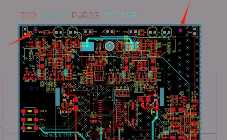
- Placement: position fiducials near the board edges, about 3 mm from the edge, so machines can easily detect them without interfering with component placement.
Final reminder
Many designers focus on routing and component layout but forget fiducials, only realizing the omission when the factory reports production or placement issues. Adding standard fiducials during the final design steps takes only minutes and prevents significant problems later. The last mile of PCB design often lies in these small details.