PCI Express, abbreviated as PCIe, is a high-speed serial computer expansion bus standard. PCIe is a high-speed serial, point-to-point, dual-simplex, high-bandwidth interconnect. Each connected device is assigned dedicated lane bandwidth and does not share bus bandwidth. Its main advantage is a high data-transfer rate.
Main Differences Between PCIe 2.0 and PCIe 3.0
1. Maximum data rate
PCIe 2.0 provides a maximum data rate of only 5 GT/s, while the PCIe 3.0 data rate reaches 8 GT/s, which increases bus bandwidth. The PCIe 3.0 specification raises the data rate to 8 GT/s and remains backward compatible with PCIe 2.x/1.x, continuing to support the 2.5 GT/s and 5 GT/s signaling schemes.
2. Encoding method
PCIe 3.0 operates at 8 GT/s and drops the traditional 8b/10b encoding. It introduces several techniques, including enhanced signaling, data integrity, transmitter and receiver equalization, PLL improvements, clock-and-data recovery, and common extensions.
Because PCIe 2.0 and PCIe 3.0 have different characteristics, they also have different PCB design requirements.
PCIe Interface PCB Design Notes
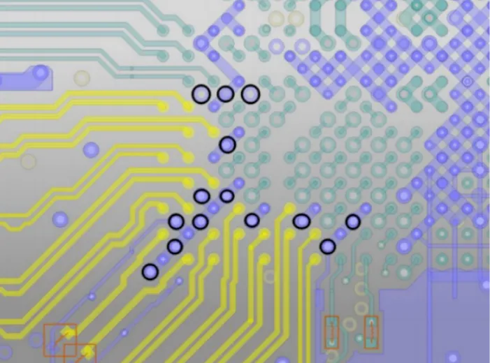
Ground vias are recommended at the following locations in the BGA region. Differential signals should also be ground-guarded, with ground-via spacing on the guard traces less than 300 mil, as shown in Figure 1.