PCI Express (PCIe) is a high-speed serial computer expansion bus standard used to connect processors, graphics cards, storage devices, network adapters, and other peripheral hardware. Unlike traditional shared-bus architectures, PCIe uses point-to-point, full-duplex serial links. Each connected device communicates through a dedicated link, allowing data to travel in both directions simultaneously.
PCIe is widely used in modern computers, embedded systems, industrial equipment, and high-performance electronic devices. Its high data transfer rate makes it suitable for applications that require fast communication between processors, memory systems, storage, and peripheral devices.
However, higher-speed PCIe interfaces also introduce stricter PCB design requirements. The routing of differential pairs, impedance control, via transitions, return paths, and signal integrity can all affect link performance.
This article compares PCIe 2.0 and PCIe 3.0 and explains the key PCB layout and routing considerations for reliable PCIe interfaces.
What Is PCI Express (PCIe)?
PCI Express is a high-speed serial interconnect standard designed for communication between a host processor and peripheral devices. It uses differential signaling, in which each signal is transmitted through a pair of conductors carrying complementary electrical signals.
A PCIe link consists of one or more lanes. Each lane includes:
-
One differential pair for transmission (TX).
-
One differential pair for reception (RX).
Because PCIe supports full-duplex communication, the transmit and receive paths can operate simultaneously.
PCIe Link Width
PCIe links are commonly described using lane widths such as x1, x4, x8, and x16.
|
PCIe Link |
Number of Lanes |
Typical Application |
|---|---|---|
|
PCIe x1 |
1 |
Network cards, expansion controllers |
|
PCIe x4 |
4 |
NVMe SSDs, storage controllers |
|
PCIe x8 |
8 |
High-performance adapters |
|
PCIe x16 |
16 |
Graphics cards and accelerator cards |
Each additional lane increases the aggregate bandwidth of the link. However, the actual bandwidth depends on the PCIe generation, encoding scheme, implementation, and negotiated link width.
Differences Between PCIe 2.0 and PCIe 3.0
PCIe 2.0 and PCIe 3.0 differ in several important ways, and each revision imposes different PCB design requirements.
1) Maximum data rate
PCIe 2.0 supports a maximum data rate of 5 GT/s, whereas PCIe 3.0 increases the data rate to 8 GT/s, raising overall bus bandwidth. The PCIe 3.0 specification increases signaling to 8 GT/s while maintaining backward compatibility with 2.5 GT/s and 5 GT/s link speeds.
2) Encoding and signaling
PCIe 3.0 operates at 8 GT/s and departs from the legacy 8b/10b encoding. It introduces enhanced signaling techniques and improvements in data integrity, transmit/receive equalization, PLL performance, clock-data recovery, and other extensions to support higher data rates.
PCB Design Considerations for PCIe Interfaces
Based on the differing characteristics of PCIe 2.0 and PCIe 3.0, the PCB layout and routing practices should be adjusted accordingly.
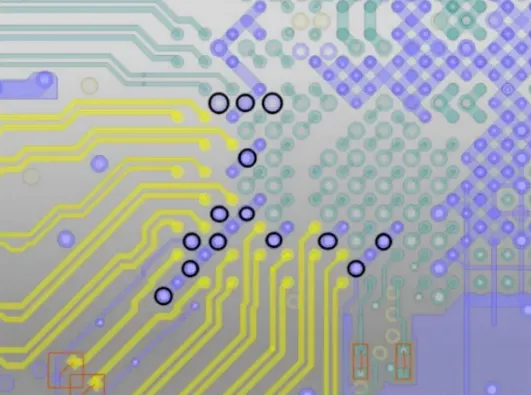
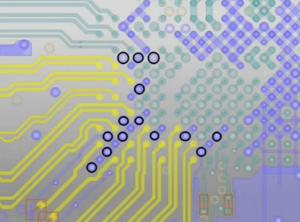
For BGA breakout and device fanout, it is recommended to add ground vias around the BGA area at the indicated positions. Differential signals should be surrounded by stitched ground (ground shielding), and the spacing between ground vias in the shield should be less than 300 mil. See Figure for an example of PCIe 3.0 BGA fanout routing.