










Introduction
In electronic products, the power module acts as an "energy manager", converting unstable power into the stable voltages required by the device. PCB design provides the physical environment for that manager to operate efficiently. Poor design can cause unstable supply, frequent crashes, and electromagnetic interference that degrades overall performance. This article covers PCB design for switching regulators and linear regulators (LDOs), explaining basic principles and practical rules so beginners can follow along.
1. Core power types: Switching Regulators and LDOs
1.1 Switching Regulators: Efficient DC-DC Converters
Switching regulators are the main power solution in many devices, performing DC-DC conversion and providing functions such as startup, overcurrent/overvoltage protection, and noise filtering. Their core is a high-speed switching action that controls the average output voltage.
The operation is like an intelligent faucet: a voltage divider monitors the output and feeds a comparator. The comparator and a PWM stage adjust the duty cycle of the power device. If the output is high, the duty cycle is reduced; if low, it is increased. This dynamic adjustment keeps the output at the target voltage.
1.2 LDO: Quiet Voltage Dropper
An LDO, or low dropout linear regulator, only reduces voltage (for example, 5 V to 3.3 V). It cannot boost voltage. Its advantage is low output ripple and simplicity, making it suitable for sensitive, low-current circuits such as sensors and microcontrollers. An LDO uses a pass device to drop excess voltage directly, so it does not generate the switching noise typical of switching regulators.
2. Switching Regulator PCB Design: Key Rules
The primary goals for switching regulator PCB design are to minimize interference and conduction losses. Always follow the component manufacturer's datasheet recommendations. The rules below summarize common practical guidelines.
2.1 Start with the datasheet and follow recommended layout
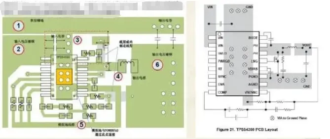
Before design, download and study the switching regulator IC datasheet. The datasheet usually provides a recommended layout and routing that is critical to avoid design mistakes. For example, layout rules for devices such as the TPS54550 are representative and can guide similar parts.
2.2 Clear main power path; place core components centrally
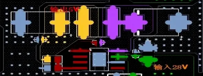
Plan the main input and output current paths so copper pours and vias are available and traces do not take long detours. Layout should center on core components such as the regulator IC and the inductor, with supporting components placed close by. Keep input and output filter stages physically separated when possible to prevent input noise coupling into the output.
2.3 Compact layout; minimize trace length and vias
Arrange components compactly, often in a linear "one-line" layout so parts are evenly distributed. Shorter traces and fewer vias reduce current loss and EMI risk. Place critical bypass and filter capacitors exactly as specified in the datasheet; moving them can degrade performance.
2.4 Heavy-current traces: use solid copper pours or wider traces
High-current traces, such as common ground and power input/output, should be handled with copper pours. If pours are not possible, increase trace width to lower resistance and reduce voltage drop. Wider traces and pours also reduce the risk of parasitic coupling that can cause instability. For low-current signal interconnects inside the module, use at least 10 mil trace width where practical, but avoid making traces wider than component pads that would cause soldering issues.
2.5 Careful handling of special pins
Certain pins require special attention to avoid introduced errors and interference:
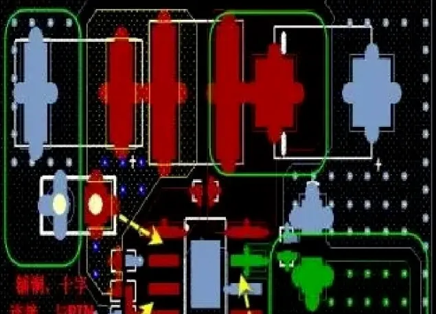
- SENSE pin: This pin senses the output voltage. Route its trace away from noisy sources and large current planes. Do not tie it directly to the switching IC pin via long or noisy traces. Use a narrow trace (about 0.5 mm) from the output filter to the sense point so the measurement reflects the true output voltage.
- GATE pin: The gate drives the power device. Keep the gate trace short and wide to reduce delay and susceptibility to interference. Route it away from noisy areas.
- INTVCC pin: The decoupling capacitor for INTVCC is critical. Place decoupling capacitors as close to the IC pin as possible so the gate driver has a low-impedance source for fast current demands.
2.6 Thermal and EMI considerations: avoid signal traces under switching parts; place inductors vertically
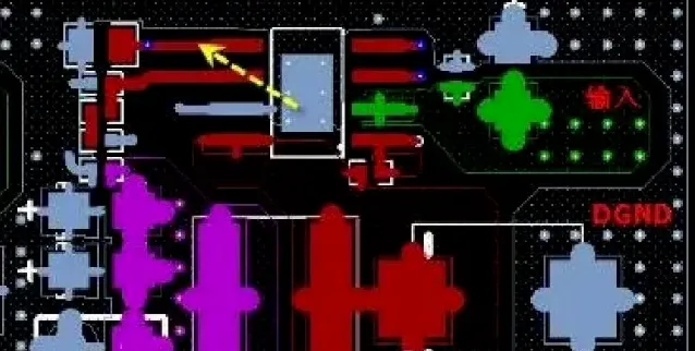
- Do not route any signal traces under the switching regulator IC or the inductor, as those areas are subject to strong switching fields and can corrupt nearby signals. Provide thermal vias in the IC thermal pad and open copper windows to ensure heat transfers into the ground plane for proper dissipation.
- For multi-output regulators, place adjacent inductors perpendicular rather than parallel. Parallel inductors can couple and interfere, causing unstable outputs.
2.7 Copper pours: leave thermal paths for soldering
Copper pours increase current capacity but avoid fully connecting every plane without thermal relief. If thermal reliefs or isolation paths are not planned, reflow soldering can cause tombstoning, solder bridging, or poor solder joints. Design pours with appropriate thermal reliefs and via patterns so heat distributes evenly during soldering.
3. LDO PCB Design: Simple But Detail-Oriented
LDO circuits are simple, but correct PCB implementation is essential for stable outputs. The following two points apply for a typical 5 V to 3.3 V LDO.
3.1 Filter capacitors: place large to small, close to pins
Place input and output capacitors in the order "large first, then small," and place them as close to the LDO input and output pins as possible. This combination filters noise across a broad frequency range and stabilizes the voltages.
3.2 Grounding: wide copper and multiple thermal vias; tie input and output grounds
Ensure the LDO ground pin connects to a wide copper pour with sufficient vias comparable to the input and output via count. This lowers ground resistance and reduces ground noise. Connect the input ground and output ground to a common ground plane to avoid ground potential differences that could cause output instability.
Summary
Power module PCB design follows the principle "follow the theory, focus on details." For switching regulators, prioritize EMI control, conduction losses, and thermal management. For LDOs, prioritize filtering and proper grounding. By following the IC datasheet and carefully implementing layout, routing, and copper design, the power module will operate reliably and provide stable power to the rest of the system.






