After GND is poured, the board looks more complete. Why does DRC still flag isolated copper? The issue is not whether the copper is shown in green. It is whether the copper is truly connected to the ground net. Small copper pieces cut out by pads, traces, and cutouts may still be named GND, yet they can be nothing more than a floating conductor on the board.
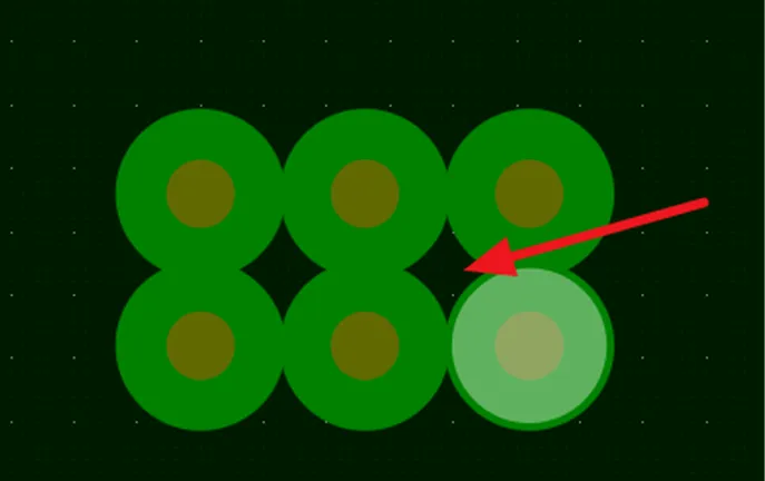
Isolated copper appears most often between BGA pads, at board edges, on both sides of dense routing, and near irregular cutouts. When you zoom by eye, it looks like part of the plane. Turn off other layers and highlight the net, and you find no via, no neck, and no continuous copper tying it back.
The engineering judgment is direct: keep copper that can form a low-impedance return path. Fragmented copper whose connection value cannot be demonstrated is usually safer to delete.
The same net name is not the same as an electrical connection
EDA tools allow objects to be assigned a net first, then compute the actual shape from clearance and pour rules. Once a local region is cut off by antipads or keep-out areas, it may still display GND without a DC connection.
A multimeter on the finished board will find the problem, but a more efficient layout-stage method is net highlighting, single-layer display, and unconnected-copper checks. Looking only at color or the property pane makes it easy to treat "same name" as "connected."
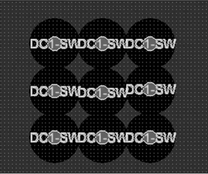
If isolated copper is tied back only by a very thin neck, DC continuity is not enough. High-frequency return current cares about impedance. The parasitic inductance of a long, thin connection can make that copper behave as if it were floating at high frequency.
When judging connectivity, also watch pour priority. Overlapping polygons, local rule overrides, or a change in pour order can disconnect a region that was previously tied together after one edit. Version review should compare not only traces, but also connectivity after the pour is recalculated.
Negative and positive layers have different display logic, so the inspection method must change with them. The final judgment still returns to electrical connection: through which vias and layers this copper ties to main ground, not the fill color on the screen.
Floating copper cannot carry a stable return path
When a signal edge passes nearby, isolated copper is coupled through parasitic capacitance. Its potential is not fixed at zero. It follows the surrounding electric field. Area, shape, and distance to the reference plane all change the coupling result.
This kind of copper island usually does not cause an immediate logic error. It can still change local impedance, crosstalk, and radiation. Long, thin slivers and fragments near the board edge or a connector are especially likely to become uncontrolled high-frequency structures.
Do not describe every isolated copper piece as an antenna. Do not treat it as effective shielding either. Without a defined ground point and return function, what it provides is uncertainty.
If high-speed traces run near isolated copper, the first concern is whether the reference environment has changed. Parasitic coupling between the copper piece and the reference plane varies with layer spacing and area. "It carries no DC current" does not cancel the high-frequency effect. When the structure is sensitive, confirm with a field solver or impedance simulation.
The larger the isolated copper area, the less it can be dismissed with "it is GND anyway." Larger area means stronger coupling and a greater chance of changing the field around nearby traces. If it is kept, give a clear grounding and functional reason.
Narrow necks and sharp corners should be cleaned up as well
To dodge pads and traces, the pour algorithm may leave very narrow necks, sharp corners, and crescent-shaped fragments. They are sometimes still connected, yet hard to manufacture, and after etching their width and shape are more likely to deviate from the design.
Cleanup should not stop at checking Remove Dead Copper. Also set a reasonable minimum copper area, minimum neck width, and cutout boundary so the pour stays clean after it is recalculated.
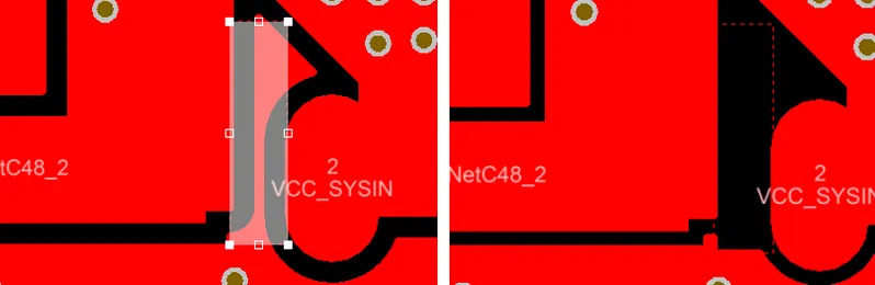
If deleting a piece of copper would break a thermal or shielding goal, reconstruct the connection first: move the obstacle, widen the neck, or add a suitable ground via. Do not keep the fragment by force.
Manufacturing also cares about copper distribution and etch uniformity, but uncontrolled fragments should not be kept just for copper balance. When copper balance is needed, use a regular copper fill or process pattern and confirm it with the fabricator. Do not let routing gaps generate copper islands of arbitrary shape.
Sharp corners themselves need not be treated as a special mystery. When a sharp corner and a thin neck appear together, they usually expose a constrained pour and insufficient process margin. Improving geometric continuity is more valuable than debating a single angle.
If the copper must stay, stitch it with vias
If a larger GND copper area truly provides shielding, heat spreading, or return current, stitch it to the adjacent ground plane with vias. Place the vias around the current path. Do not fill them mechanically just to look uniform.
There is no universal via pitch independent of frequency, stackup, and structure. During review, confirm that each via belongs to the correct net, reaches the target ground layer, and is not isolated by an antipad or a layer setting.
Finally, re-pour copper, run DRC, and highlight connectivity again. The work is finished only when every copper piece can be described by its connection points, purpose, and return path.
Stitching vias must also avoid "logically grounded, physically detoured." If a via lands only on a local copper island and then travels a long path before reaching main ground, the connection is still poor. Tracing via landings and plane continuity through the stackup is more reliable than counting vias.
After vias are placed, recheck solder mask, pad clearance, and manufacturability. Inserting vias that cannot be fabricated or that sit too close to component pads only trades one problem for another.
Conclusion
The value of a copper pour is not coverage. It is a controlled current path. Isolated copper, thin necks, and fragments that cannot perform a defined return, thermal, or shielding task are not worth keeping.
After the next pour, turn off other layers and find isolated regions piece by piece, then decide whether to connect, reconstruct, or delete. That action matters more than watching whether the whole-board copper looks "full."
After isolated-copper checks are added to the review list, run them again after every part move, differential-pair adjustment, and cutout change. Isolated copper does not appear only after the last pour. It reappears as local clearances and rules change.