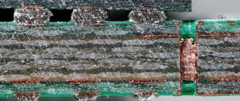
The shape of an oblong slot, the cutter path, and the plating attribute are not the same class of data. Drawing an outline on the mechanical layer does not replace an NC Route output, and it does not automatically tell the fabricator whether the slot wall needs to be plated.
A connector footprint may already contain a clean oblong slot, and the 3D view may show no interference. The boards that come back can still have the wrong slot width, unplated walls, or a feature treated as an ordinary outline notch. These problems are often not missing geometry. They are manufacturing data that never fully stated the process intent.
A mechanical-layer outline only answers "what is the shape." It does not automatically answer "what cutter path should be used" or "whether the wall is plated." Before release, the slot-routing file, pad attributes, and fabrication notes must say the same thing.
Start from the machining command, not only the mechanical layer
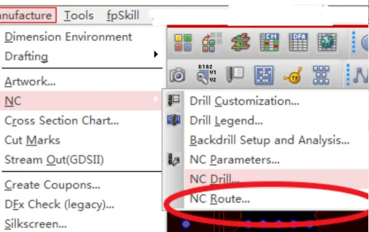
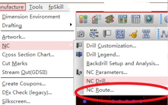
In Allegro manufacturing output, slot milling paths are generated by NC Route commands. That is not the same as a wireframe on the outline layer. The wireframe helps people understand the feature. The route file is the primary input CAM uses to generate the cutter path. This is why mechanical features should be considered part of the broader PCB fabrication workflow rather than isolated CAD geometry. Once the manufacturing package is released, the design data must be interpreted, checked in CAM, and translated into routing, drilling, plating, and inspection operations. Understanding this transition helps designers identify manufacturability risks before production begins.
If the footprint library contains only a mechanical outline, the factory must make a further human judgment from the fabrication notes. Small-volume jobs may be queried back by engineering. Highly automated flows may apply default rules instead.
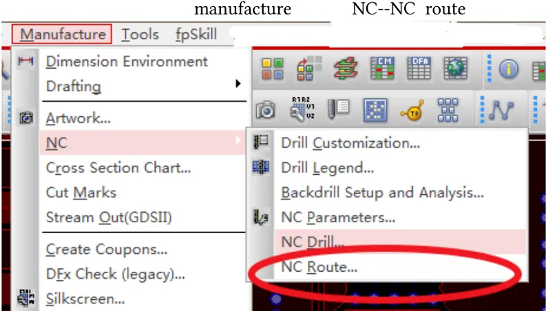
Seeing an outline does not mean CAM sees an executable cutter path.
Check units and output parameters together with the route file
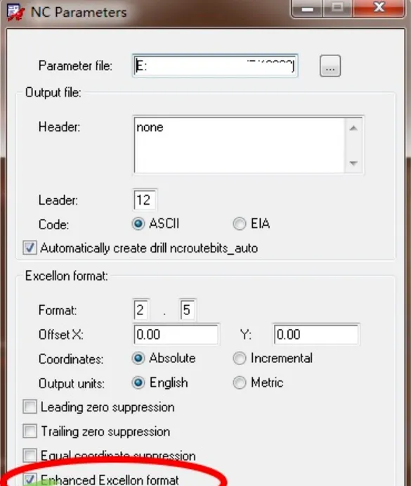
In the output dialog, file name, route type, units, and numeric format all affect later parsing. Even if the slot location is correct, units or precision that do not match the rest of the Gerber set can produce scale, coordinate, or size errors in CAM.
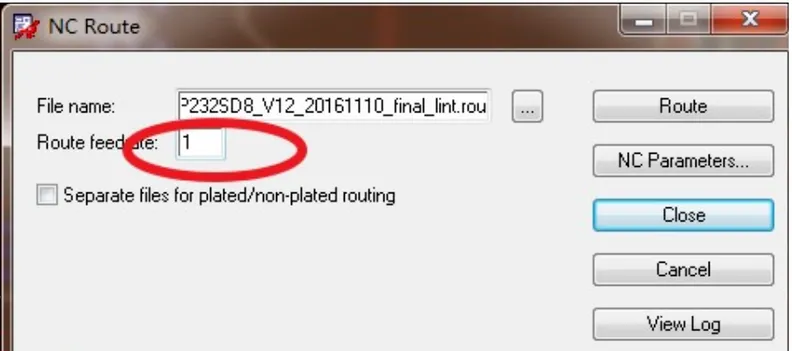
Do not stop at confirming that "the file was generated." Open the output log, then overlay the route layer with drill and outline data. Confirm that slot center, length, width, and opening direction have not shifted.
Plated and non-plated slots differ by more than a drawn outline
Slots used for through-hole pins usually need to be soldered. Mechanical latch slots may not need plated walls. The two outlines can be identical, but pad attributes, slot classification, and process results are completely different.
In library management, bind length, width, annular ring, and plating status to the device drawing. If only the outline is copied and the hole attributes are not, dimensional checks rarely catch the error. It shows up later in soldering or reliability.
The same oblong shape can correspond to two completely different manufacturing results.
These distinctions are not only theoretical. In real PCB manufacturing, non-plated slots can create CAM clarification issues when their dimensions, plating intent, or routing requirements are not fully defined in the production data. AIVON's DFM case on non-plated slots, gold fingers, and trace extensions shows how these issues can be identified and resolved during CAM review before the board enters production.
CAM review must confirm that the file actually arrived
Seeing only a layer name in CAM after export does not mean the content is correct. Zoom to each slot and check whether it is a closed path or a centerline cutter path, whether it is concentric with the pad and solder-mask opening, and whether the route start and end points contain extra segments.

The file list must also confirm that the route file was not omitted during packaging and that its version matches the current Gerbers. Mixing different versions of outline, drill, and route data is harder to debug than a single incorrectly drawn slot.
Use a four-way cross-check before release. Put the device drawing, PCB footprint attributes, NC Route output, and CAM overlay on the same checklist. The drawing states finished size. The footprint states electrical attributes. The route file states the cutter path. CAM states what will actually be delivered.
If plating on a particular slot is critical to reliability, add a reference designator or coordinates in the fabrication notes. Do not let "fabricate per drawing" replace information that can be checked. The more unique the data sent out, the less the fabricator has to guess.
Slot size must also state whether it is finished size or cutter centerline. For an oblong slot milled with a router bit, tool-diameter compensation determines the finished boundary. If the design side provides only a line and does not state how it should be interpreted, different CAM rules can produce different widths. During inspection, measure the finished boundary, not only the centerline.
The relationship between pads and slots also cannot rely on visual inspection alone. A plated slot needs enough annular ring and solder-mask opening. A non-plated slot must avoid unintended connection to nearby copper. Compare pin function against the package drawing, then inspect the actual copper ring, solder mask, and cutter path in CAM to confirm whether the feature is a solderable pin or pure mechanical location.
Slots on panelization features and board edges are easier to confuse with outline routing. If a slot happens to intersect the board frame, CAM may merge it into the outline cut. Check the single-board outline, panel ties, process rails, and slot layer together so a feature that looks correct in the single-board view is not rewritten in the panel data.
The most effective manufacturing closed loop is one in which the fabricator does not need to ask "how should this slot be made." Put a single-version cutter-path file in the release package, call out critical plated slots in the fabrication notes, and use CAM comparison plots for internal sign-off. That set of actions reduces misunderstanding more than thickening the outline on the mechanical layer.
If a company has its own footprint library rules, split long slots into two controlled templates: plated oblong slots and non-plated oblong slots. Fix hole attributes, pad relationships, solder-mask rules, and manufacturing output class in the template. Users change only the dimensions from the device drawing. When a footprint is released, run a representative part with plated slots through NC Route and CAM acceptance and keep a complete review record. That is more controllable than drawing lines ad hoc on every project.
Conclusion
Slots are often fabricated incorrectly not because the mechanical-layer line was missing, but because outline, cutter path, and hole attributes never reached the same conclusion.
Before the next release, do not only open the Gerbers and glance at the outline. Make the route layer, drill layer, and pads visible together in CAM. Only then is the manufacturing intent of the slot truly closed.
For designers dealing with complex mechanical features, slot definition is only one part of the CAM review process. Hole attributes, special drilling, panelization, edge machining, and other manufacturing features can create similar data-interpretation conflicts. See AIVON's CAM Review Cases for more examples of manufacturability issues identified before production.