The reference designator is clearly present in the Gerber, yet the finished board shows only half a character. The usual cause is not a missed print at the factory. It is silkscreen that entered a solder-mask opening. To keep exposed pads solderable, manufacturing often deletes the overlapping ink on purpose. The effective fix is to control the relationship between silkscreen and openings at the footprint and DRC stage, so polarity marks, pin 1, and reference designators stay readable without invading solderable areas.
After boards return, R37 may show only an "R," and the pin-1 triangle on a connector may be missing a corner. Designers often treat this as a silkscreen accuracy problem. Overlay the finished board with the Gerber, and the missing region often sits right against a pad edge. The issue is not whether the character was drawn thick enough. It is whether the silkscreen layer crossed the solder-mask opening boundary.
What is missing is not the artwork. Process is yielding to solderability
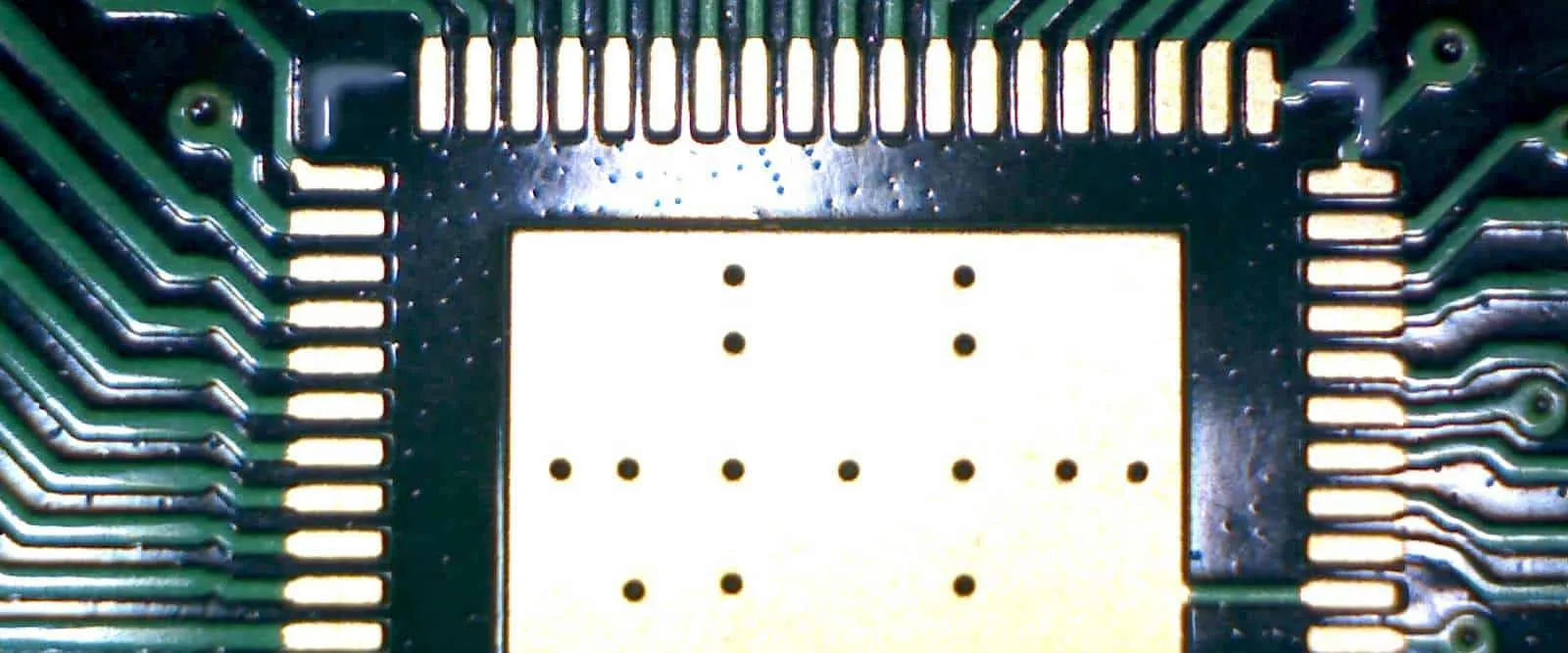
Pads need exposed copper. Solder-mask openings create the solderable area. Silkscreen ink can land only where printing is allowed. When the two overlap, ink left on the pad surface can contaminate the solderable area and degrade joint appearance and inspectability. Manufacturing usually keeps the pad and clips the conflicting silkscreen. The character is complete in the file and broken on the finished board.
That also explains why some characters on the same board are intact and others are incomplete. The whole-board print did not shift. Only local features next to openings triggered the clip. If an ordinary reference designator is removed, assembly and repair identification suffer. If polarity, connector orientation, or a pin-1 mark is removed, the consequence is more immediate.
Rules must constrain solder-mask openings, not only copper
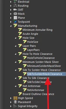
In Altium Designer, Silk To Solder Mask Clearance is available among the manufacturing rules. The name already states the comparison: silkscreen must clear the solder-mask opening, not only the copper outline. Some pads have solder-mask expansion larger than the copper pad. If you leave a gap from copper by eye only, silkscreen can still enter the opening.
Rule scope also needs care. Constraining only text on Top Overlay while omitting lines, polarity symbols, or Bottom Overlay in footprints still leaves DRC blind spots. A more reliable approach is to include every silkscreen object that will be exported for production, then set minimum clearance from fabricator capability and company rules. Without a common process basis, do not copy a fixed value that only looks conservative.
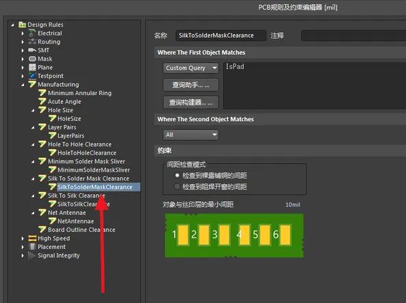
Turn on both online hints and batch DRC
Creating the rule does not mean it is in effect. The corresponding manufacturing check must also be selected in the design rule checker so batch DRC can produce a violation list. Online DRC is for immediate feedback during placement. Batch DRC is for a full-board sweep before release. They solve different stages. Online hints alone can leave conflicts that already exist in old footprints untouched. Batch checking only at the end piles large numbers of reference-designator moves onto the delivery date.
Do not delete silkscreen for every error. A reference designator can move to empty space near the part. A polarity mark must keep its directional relationship. In dense areas, shorten a line or change the mark style. If space is truly insufficient, assembly identification can go on an assembly layer, but the board face used for repair should still keep enough critical markings.
When characters are missing on the finished board, trace three layers
Start from where the finished gap lands. Check whether it intersects a pad or test-point solder-mask opening. Then return to the footprint and check silkscreen origin, rotation, and mirroring. Then open the Gerber and confirm the output layer against the manufacturing clip. That separates design conflict, output error, and true print offset.
Gerber review cannot be a single-layer screenshot. Overlay top silkscreen, top solder mask, and copper, then zoom to connectors, fine-pitch ICs, test points, and parts at the board edge to see the real relationship after opening expansion. Panelization, mirroring, and version replacement can also move a previously safe mark next to a new pad. After an engineering change, rerun manufacturing DRC. Do not reuse the previous lot's check conclusion.
The footprint library is the best place to fix this once. If common passives, ICs, and connectors already place reference designators, pin 1, and outline lines in a safe region, new projects avoid a large number of repeated edits. For fine-pitch parts, open copper, solder mask, and silkscreen together during library review. Do not judge Overlay alone by whether it "looks neat."
Release notes should also state priority: when the fabricator finds a conflict, may ordinary reference designators be deleted, or must polarity and orientation marks be sent back for confirmation? If design gives no rule, manufacturing can only follow general solderability practice. Keep a list of critical markings under version control so the same board does not receive different silkscreen results at different factories.
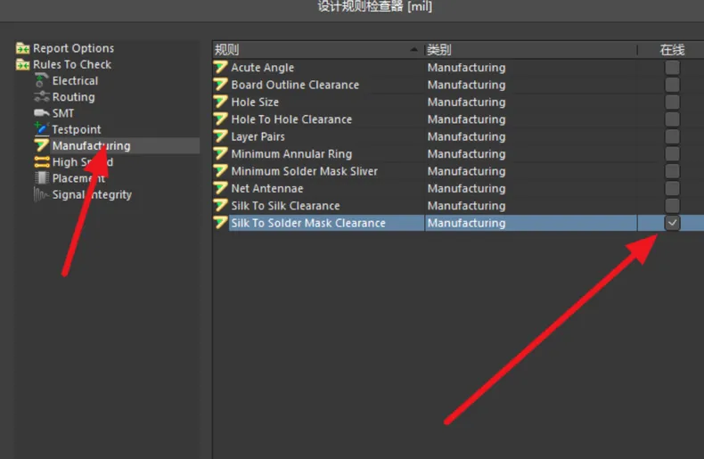
The criterion is simple: silkscreen must yield to solderability, but critical identification must not be decided by random clipping at the factory. Expose the conflict in DRC first, and every character on the finished board becomes predictable.