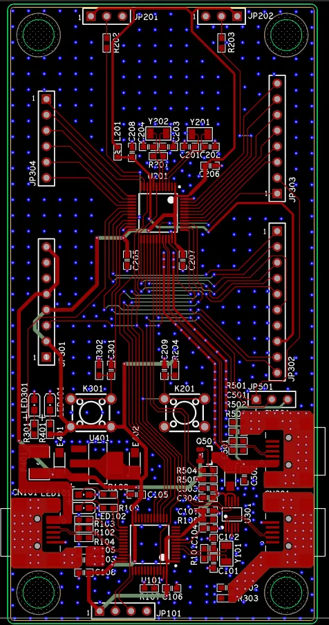
Recently, as large models have become more capable, there have been demonstrations of AI directly operating KiCad to complete PCB design.
Many PCB engineers have begun to worry: will AI eventually replace PCB engineers?
My assessment is:
PCB engineers will not be entirely replaced by AI, but the role will be redefined.
The first to be affected will be the part of the job that only involves operating software and "drawing the board."
AI is shifting from "telling you how" to "doing it for you"
Previously, AI mostly answered questions: How should high-speed traces be routed? How to handle differential pairs? What to consider for power distribution?
Now it is different. AI has started to enter EDA tools and directly execute design tasks.
This means many rule-based, repetitive tasks may gradually be handed to AI, such as basic placement and routing, repeated modifications, rule checking, documentation, and version adjustments.
These tasks are essentially execution-oriented. As long as the rules are clear, AI will become increasingly proficient.
So if a PCB engineer's core competence is only:
Being very familiar with AD;
Being very familiar with PADS;
Being very familiar with Allegro;
Someone hands me a schematic and I just draw the board;
then there should indeed be some concern.
"Knowing how to draw a PCB" is not the same as "making the product work"
The hardest part of a real project is rarely how to operate the software. Often, the engineer must judge what the rules should be in the first place.
Real projects often look like this:
The mechanical structure is fixed;
Cost cannot increase;
Space is very tight;
Delivery schedules are tight;
The design must pass EMC;
Performance, manufacturability, and reliability conflict with each other.
At that point, the real question is not "How to route this trace?" but rather:
How should the board be designed overall?
You must judge:
What is most important? Where are the highest risks? Which aspects are nonnegotiable and which can be compromised? Why must this component be located here? Why can this trace not be routed that way? If the board has problems after fabrication, where should you start troubleshooting?
These abilities cannot be obtained by merely being proficient with EDA tools. What is required is engineering judgement.
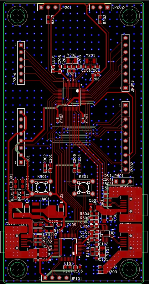
PCB engineers will likely split into three levels
Level 1: Standardized tasks handed to AI.
Basic placement, partial routing, checking, modifications, and documentation will see increasing AI involvement.
Level 2: AI designs first; engineers review and optimize.
Engineers may not route every trace by hand, but they must understand why critical traces are routed a certain way.
Level 3: For complex projects, engineers define constraints and make technical decisions.
AI can search for solutions based on rules, but someone must first tell it what the rules are.
This is the true value of a high-level PCB engineer.
AI may not eliminate PCB engineers, but teams will shrink
Previously, a project might require several people to complete. In the future, one experienced engineer with AI may accomplish the workload of several people.
Therefore, expectations for PCB engineers will not decrease; they will likely increase.
Companies will no longer pay only for "fast board drawing." They will pay for someone they can trust to take responsibility for the board.
You must understand the product, define constraints, anticipate risks, find problems in AI-generated solutions, and continue troubleshooting if issues appear after fabrication.
This is the real value of an engineer.
So the focus of learning PCB should change
Of course learn the software. But do not spend all your energy on where a button is, which shortcut to press, or how to drag a trace.
Ask yourself instead:
Why is this layout chosen? Why must this trace be routed this way? What problem does this rule solve? If conditions change, does the rule still hold? If the board fails, can I locate the cause?
AI will first replace the parts of PCB work that do not require judgement.
Conclusion
The most valuable PCB engineers in the future will not be those who can out-draw AI. They will be those who understand better than AI why the board must be drawn that way.
Competition will not be limited to software proficiency. It will be about who understands the product, constraints, risk assessment, how to use AI effectively, and who can ultimately solve real engineering problems.
I am not pessimistic about the PCB engineering profession as a whole. However, people who only operate EDA tools and lack engineering judgement will face increasing pressure from AI.
Do not compete with AI on who draws boards better.
Become the person who knows why the board must be drawn that way.