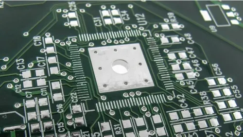
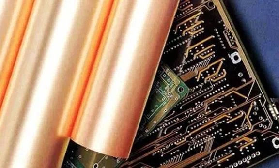
In production we handle FR4 PCB ENIG defects, especially ENIG black pad, by keeping the electroless nickel and immersion gold baths inside narrow chemical windows and rejecting any panel that shows abnormal nickel corrosion or uneven gold color during in-line checks. CAM engineers do not redesign the finish stack-up; the plating line owns the problem. Daily XRF thickness maps, bath analysis, and sample cross-sections decide whether a lot moves forward or gets held.
Why electroless nickel still corrodes on FR4 even when baths look controlled
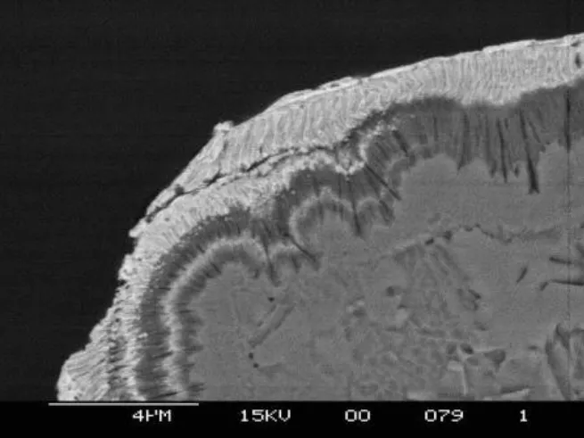
The defect appears because electroless nickel is catalytic and highly sensitive to the copper surface that arrives from the preceding processes. Residual oxide, smear from drilling, or uneven micro-etch leaves active sites that plate nickel with higher phosphorus or coarser grain. When the immersion gold bath starts displacing nickel, those grain boundaries are attacked preferentially and form the black, porous layer known as black pad. FR4 itself contributes: the resin and glass can leave local contamination after desmear, and large copper density differences across a panel change the local plating rate so edge coupons and center coupons rarely match. Bath age, hypophosphite level, and pH drift of only 0.2 units are enough to push phosphorus outside the 7–11 % range that resists gold attack. Temperature swings of a few degrees on a long panel line produce the same result. None of these factors are design issues; they are process and material realities that show up every time the line runs.
What black pad and out-of-spec nickel/gold actually do to yield and assembly
Once black pad is present the solder joint becomes brittle. Intermetallic growth during reflow is irregular, so the joint cracks under thermal cycling or mechanical stress. Assembly houses report open circuits or intermittent failures after a few hundred cycles. On the fab side we see the cost immediately: any panel confirmed by SEM or cross-section is scrapped or, at best, partially recovered by selective rework that rarely pays for itself. Lot rejection rates climb, X-ray and AOI queues back up, and shipment dates slip while we wait for new panels. Thin or porous gold accelerates the same problem by allowing nickel oxidation before the board even reaches the customer. Thick gold, on the other hand, can trap contaminants and produce dull appearance that customers reject on visual inspection. Either way the panel leaves the line as scrap or delayed product.

Process windows and checks we actually run to keep nickel and gold in control
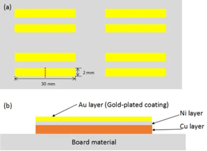
We keep nickel thickness between 3 µm and 6 µm with panel uniformity better than ±0.5 µm, measured by XRF at five or more locations per panel. Gold stays at 0.05–0.1 µm. These numbers are not customer preferences; they are the range where black-pad risk stays low on FR4. Every shift the plating engineers sample nickel concentration, sodium hypophosphite, stabilizer level, and pH (held 4.5–5.0). Temperature is locked at 85–90 °C. Pre-treatment micro-etch is adjusted daily so the copper surface is uniformly active before nickel starts. Immersion gold time and free-cyanide level are trimmed so the displacement reaction does not over-attack the nickel. After plating we run AOI for color uniformity and pull sample coupons for cross-section grain structure. When a bath starts to age we either dump or add stabilizer rather than push it past the point where black pad appears. Panel design helps indirectly: we ask CAM to avoid extreme copper density gradients that create local rate differences, but the real control stays on the wet line. These steps are used because electroless processes have no external current to correct local chemistry; the only levers are bath composition, time, and temperature.
When thinner nickel or higher gold risk is accepted on non-critical FR4 boards
For consumer boards that never see thermal cycling and use large pads we sometimes drop the nickel lower limit to 2.5 µm or allow gold up to 0.15 µm if the customer signs the risk. Prototype or very low-volume lots can skip full daily bath titration when the line has been stable for several days, but XRF thickness mapping is never skipped on production material. The trade-off is clear: lower process cost and faster turnaround against higher probability of field returns. High-reliability, fine-pitch, or automotive boards stay inside the full control window with no exceptions.