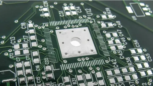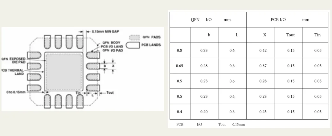
Extending QFN peripheral pads outward leaves room for soldering and inspection. Extending them inward consumes the clearance to the center thermal pad. Tin and Tout in the package dimension table must not be treated as a single total length that can be allocated at will.
To make solder joints easier to inspect, QFN peripheral I/O pads are usually extended beyond the package terminals on the outside. Seeing the benefit of that outward extension, some designers lengthen both ends of the pad in the hope of a more robust joint. After reflow, fine solder bridges appear between the peripheral pins and the center thermal pad, and visual inspection often misses them.
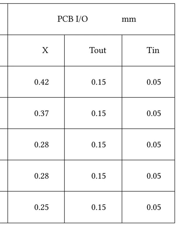
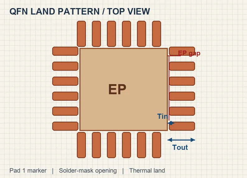
The two directions must be treated separately: Tout faces the outside of the package; Tin faces the center thermal pad. Outward extension mainly improves fillet formation and inspectability. Inward extension directly consumes electrical clearance, solder-mask dams, and solder-paste process margin. The two cannot be summarized as "longer pads are better."
Start with the three boundaries in the recommended land pattern
A recommended QFN land pattern usually specifies peripheral pad width, outward extension, inward extension, and the maximum extent of the center thermal pad at the same time. The dashed package outline, terminal outline, and PCB copper each have a meaning. Do not measure a single overall length and then center the pad in the EDA tool.
The center thermal pad is not an ordinary empty area. It provides heat dissipation and grounding, and it often has its own solder-paste windowing. Extending the peripheral pads farther inward reduces more than copper-to-copper distance; it can also leave the solder-mask dam and the stencil aperture without remaining margin.
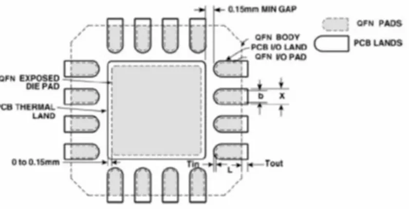
Package review must look at directional dimensions, not only total pad length.
Tin is not a substitute for insufficient Tout
Example tables in the documentation split Tout and Tin into two columns. At the same pin pitch, PCB pad length may vary, but the outward and inward extensions still serve different goals. Moving the visible fillet length needed on the outside to the inside does not produce the same inspectability.
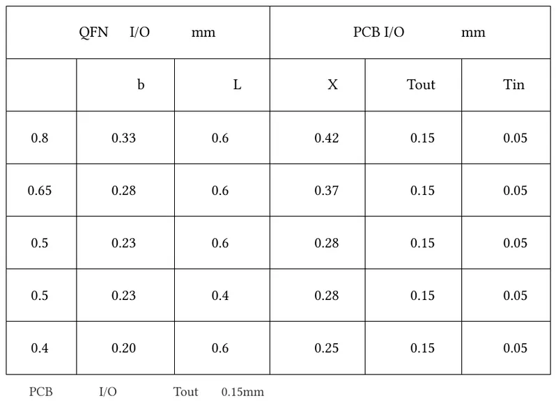
When package terminal length has tolerance, inward extension only needs to guarantee reliable overlap between the terminal and the pad. Excessive inward extension cannot be seen from the outside of the package and also brings solder closer to the center thermal pad. Follow the current recommended land pattern for the target device rather than copying a single library rule of thumb.
Bridging risk also depends on how the solder paste is apertured
Acceptable copper clearance does not guarantee a safe reflow result. If the center thermal pad is opened as a single stencil window, excess paste volume can be squeezed outward when the package is placed. If the peripheral I/O pads also encroach inward, the two conditions stack during reflow.
How solder mask is defined also changes the effective isolation. A solder-mask dam that is too narrow may merge in manufacturing, and aperture misregistration can expose more copper edge locally. During review, copper, solder mask, and stencil must be stacked and inspected together, not signed off as three independent rule checks.
Bridging is not caused by copper spacing alone. It is the combined result of copper, solder mask, and solder paste.
Make the dimensions reviewable objects in the EDA footprint
When building the library, record peripheral pad-to-terminal overlap, Tin, Tout, and center-pad clearance as footprint check items. Place the pad origin where it is easy to measure, and model the center thermal pad separately so that later changes to total length do not stretch both ends equally.
If a device has multiple package versions, do not reuse a footprint based only on pin count. Differences in body width, exposed-pad size, and terminal length all change the inward remaining margin. Before releasing a footprint, overlay the device recommended land pattern. That finds manufacturing risk more reliably than checking whether the 3D models merely coincide.
Prototype verification should focus on the hardest-to-inspect region. After reflow, do not only look at fillets on the outside of the package. Use X-ray or an appropriate cross-section method to inspect around the center thermal pad. A normal appearance does not rule out fine solder bridges under the package, especially when center-pad paste coverage is high or the package warps.
After stencil thickness, paste-window ratio, placement force, or the reflow profile change, a previously safe clearance can lose its margin. A reliable footprint is not a set of attractive dimensions. It is a design in which layout, stencil, and process still pass at the same worst-case boundary.
Thermal vias in the thermal pad also change solder distribution. If vias are not plugged or the mask coverage is inadequate, paste can be drawn into the holes and the center pad can sag locally. Some areas then have too little solder, while others are squeezed toward the edge by package weight. Via process must be evaluated together with stencil windowing; confirming via count at the PCB level is not enough.
A larger center thermal pad is not always better. More copper area helps heat dissipation and grounding, but it further compresses the inward space of the peripheral I/O pads. If the recommended land pattern gives a size range for the center pad, first satisfy the minimum isolation between terminals and the thermal pad, then consider improving thermal performance with copper expansion, inner-layer connections, or thermal vias.
Solder-mask expansion and paste reduction in the footprint library should not reuse one global default. Fine-pitch QFNs with a large center pad and ordinary chip components have different process windows. Unified parameters can make local solder-mask dams disappear. Library review should export the generated actual aperture drawings rather than only reading numbers in the property box.
Before volume production, prepare a validation board that represents minimum spacing, maximum center-pad paste volume, and the least favorable device tolerances. After reflow, record bridging, voids, and package float height, and feed the results back into the footprint and stencil specifications. What accumulates is not a patch for one project, but a boundary that the next footprint build can reuse directly.
Conclusion
Outward and inward extension of QFN pads solve two different problems. The outside is reserved for fillets and inspection. The inside must leave margin for the center thermal pad, solder-mask dams, and solder-paste flow.
The next time a footprint is reviewed, mark Tin, Tout, and exposed-pad clearance separately, then overlay solder-mask and stencil checks. Bridging risk will surface earlier than it does when only total pad length is measured.