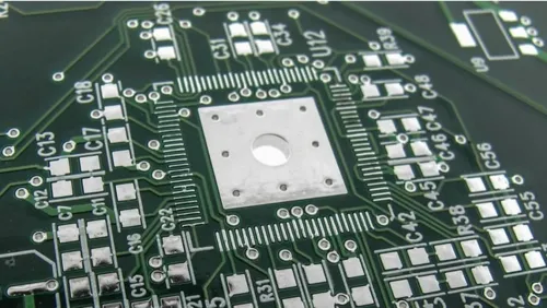
In production we treat FR4 PCB final inspection as the last hard stop before any board leaves the factory. Every lot goes through the same fixed sequence: visual appearance, outline and thickness measurement, circuit/hole/solder-mask review, electrical test, then formal quality judgment and release documentation. CAM and QA do not sign the packing list until all five stations clear against the customer Gerber set and the internal process window. That is the only rule that keeps defective FR4 boards from shipping.
What we typically see on the line is that most defects that reach final inspection are not design errors—they are process drift that built up through the earlier stages. FR4 core and prepreg still move with moisture and residual stress after lamination. Copper plating thickness varies from panel edge to center. Drill bits wear and wander. Solder mask registration shifts a few mils after the final cure cycle. These small deviations only become visible when the finished board is measured against the original data. That is why the FR4 PCB quality inspection station exists as a catch-all rather than a simple cosmetic check.
What the visual station actually rejects on finished FR4 boards
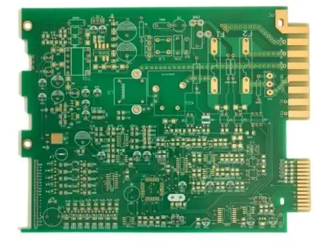
Visual inspection is still done under 10×–20× magnification with both white light and UV. Operators look for exposed copper, solder-mask voids larger than 0.1 mm, white powder residue from incomplete desmear, resin smear on pads, and any edge burr left by the routing bit. On FR4 the most common rejects are mask color variation across the panel and small copper nodules that survived the micro-etch. If these are left unchecked they reach the customer as "cosmetic" complaints that quickly turn into functional returns when the board is wave-soldered or reflowed.
From a fabrication standpoint this becomes sensitive because FR4 surface roughness and glass-weave texture change how light reflects. A defect that looks acceptable under one lighting angle can look like a crater under another. That is why we force every panel through both lighting conditions before it moves to dimensional check.
How outline and board thickness get verified before packing
Dimensional inspection is done on a coordinate measuring machine or a calibrated digital caliper set. We measure the finished outline at a minimum of four points and the board thickness at five locations—four corners and the center. For standard FR4 the thickness tolerance is typically ±10 % of the nominal value, but many customers tighten it to ±0.10 mm. Outline tolerance is usually ±0.15 mm for routed boards and ±0.10 mm for scored boards.
In production this check catches the cumulative effect of lamination expansion, plating build-up, and routing bit wear. If thickness is out, the board will not seat correctly in the customer's fixture or will create uneven pressure during assembly. If the outline is short, the board will not fit the chassis. Both cases force a full lot hold and usually a re-route or scrap decision.
Where circuit, hole, and solder-mask defects still appear after AOI
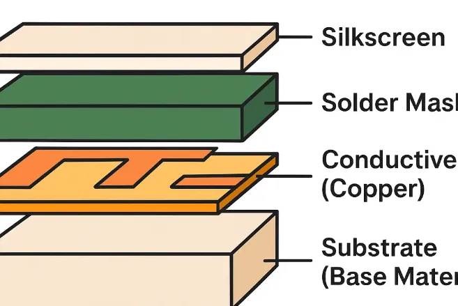
Even after AOI, final inspection still includes a manual review of critical nets, annular rings, and solder-mask registration. Operators check that minimum annular ring is still ≥0.05 mm after plating and etching, that solder-mask dams between fine-pitch pads are intact, and that no solder-mask ink has entered the via holes. On FR4 the glass weave can cause local etch variation that AOI sometimes misses if the contrast is low.
If these items are not controlled we see open vias after thermal stress, mask lift during soldering, or shorted pads when the assembly house applies paste. The yield drop shows up as customer line stops rather than internal scrap, which is why the final visual pass is still required even when AOI coverage is high.
How electrical testing and reliability sampling close the lot
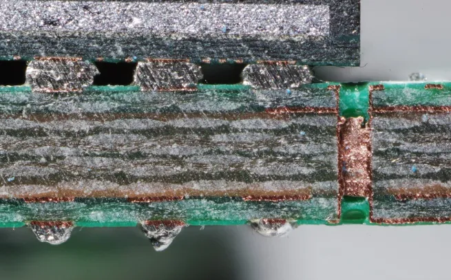
Every board that passes visual and dimensional check goes to electrical test—flying probe for prototypes and small lots, dedicated fixture for volume. Continuity and isolation are measured against the netlist extracted from the Gerber. For multilayer FR4 we also pull a sample for micro-section to verify dielectric thickness, copper thickness, and hole-wall quality. High-reliability lots add thermal-stress testing (288 °C solder float or reflow simulation) on a defined sample size.
The reason we keep both electrical and destructive sampling is that FR4 can hide intermittent opens caused by thin copper in the hole wall or by resin recession. Electrical test alone will not catch a weak barrel that fails after the first reflow. When the sample fails, the entire lot is quarantined and the plating or lamination process is reviewed before any additional boards are released.
Recording the final quality judgment and release decision
Once all stations pass, QA records the lot number, measured thickness range, electrical yield, visual reject count, and any special notes on the inspection report. That report is signed by the QA supervisor and attached to the packing list. Only then does the warehouse receive the release. If any single station fails, the lot stays in the inspection area until the root cause is identified and either rework is completed or the boards are scrapped.
Most factories will relax the visual criteria only for pure prototype runs where the customer has explicitly accepted Class 2 cosmetic standards and the electrical test is 100 % clean. Thickness and electrical requirements are almost never relaxed because those parameters directly affect assembly fit and long-term reliability. The trade-off is simple: a slightly imperfect-looking board that still meets electrical and dimensional specs can ship for engineering samples; a board that is electrically marginal or dimensionally out of tolerance does not leave the factory regardless of volume or schedule pressure.
That is how FR4 PCB final inspection is actually run on the floor. The sequence is fixed, the measurement points are fixed, and the release signature is non-negotiable. Anything less turns process variation into customer failures.