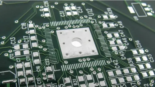
In production we treat FR4 PCB surface finish defects as a process-control problem, not a post-process salvage problem. For HASL the line runs with locked pot temperature, dwell time and air-knife pressure. For ENIG the nickel and gold baths are held to tight chemistry windows and immersion timers. For OSP the copper surface must leave micro-etch clean and the film is applied under controlled thickness and drying conditions. CAM does not redraw the finish itself, but we reject or flag any panel layout that creates large copper-density swings or pads smaller than the process window can coat uniformly. That is the standing rule on the floor.
Why finish variation keeps appearing on the plating and coating lines
Surface finish sits at the end of the process chain, so every earlier variation lands on it. After outer-layer etch the copper topography is never perfectly flat; residual resist or uneven micro-etch leaves peaks and valleys that the immersion or spray chemistry follows. On a large FR4 panel the copper density can swing from open ground planes to dense BGA fields; the local current density or solution flow rate changes with that swing. HASL adds thermal shock—the FR4 expands, the solder freezes at different rates across the panel, and the air knife cannot equalize thickness on every pad. ENIG suffers from bath drag-out and local depletion when the panel is densely populated with small features. OSP film thickness drifts if the copper surface still carries micro-oxide or if the drying temperature is uneven. Equipment tolerances on immersion tanks and horizontal coaters are typically ±5–8 % on thickness or coverage; that alone is enough to push marginal pads outside the solderability window. These are production forces, not design preferences.
What shows up downstream when the finish is left uncontrolled
Uncontrolled FR4 PCB surface finish defects move straight into assembly and customer returns. HASL that is too thin or de-wetted leaves bare copper that oxidizes before reflow; the joint fails open or forms voids. Thick HASL on fine-pitch pads creates solder bridges that the stencil cannot compensate. ENIG black-pad (hyper-corrosive nickel) or gold under 0.03 µm produces brittle intermetallics that crack under thermal cycling. OSP that is too thin or contaminated oxidizes within days, killing wetting on the first reflow pass. Final AOI or flying-probe may catch gross opens, but the real loss appears at SMT yield: 3–8 % first-pass drop is common when finish uniformity is ignored. Rework is limited—most finishes cannot be re-applied without stripping the entire outer copper—so the panel is usually scrapped. Shipment delays follow because the lot must be replaced from a new start.
How the process window is actually held on the floor
We hold FR4 PCB surface finish defects inside limits by locking the variables that move the fastest. Pre-treatment is the first gate: micro-etch rate is measured every shift and held to 0.8–1.2 µm removal so the copper surface energy stays consistent. For HASL the solder pot stays at 265–275 °C, dwell is fixed by panel size, and air-knife pressure is adjusted only after a first-article thickness map. For ENIG we run XRF on every lot—nickel target 3–6 µm, gold 0.05–0.10 µm—and reject any panel that falls outside ±15 % of the mean. Bath analysis (nickel concentration, pH, gold content, contaminant ions) is done at set intervals; if the window drifts the line stops. OSP thickness is checked by contact-angle or UV fluorescence; the film must wet uniformly and stay within the vendor’s recommended range. Panelization is adjusted so copper density variation stays under 30 % across the working area; extreme open-to-dense transitions are balanced with thieving or dummy pads. Final inspection uses AOI for coverage defects plus solderability sampling (dip-and-look or wetting-balance) on a statistical sample. Any defect that affects more than a few pads triggers a full lot hold and root-cause check on the previous process step.
These controls exist because the finish is the last chemical step; once the panel leaves the line the only remaining options are scrap or expensive strip-and-replate. Tight process windows cost less than the yield loss and customer claims that follow uncontrolled variation.
When the factory will relax the same limits
Relaxation is allowed only on low-risk designs. Large pads (>1.0 mm), coarse pitch, and single-sided boards with no fine features can run with wider thickness windows and reduced sampling. Prototype lots under 50 panels sometimes skip full XRF mapping if the customer accepts a visual-only acceptance. High-reliability, fine-pitch BGA, or long-shelf-life requirements stay under the full control plan—no exceptions. The trade-off is clear: looser control saves a few hours of inspection time but raises the chance of assembly rejects later. We document the relaxed criteria on the traveler so the decision is visible to both the floor and the customer.