










In production we treat FR4 PCB warpage and twist as two different mechanical deviations that both show up after lamination and final baking. Warpage is the simple bow—maximum distance from the highest point to the lowest point when the board is free-standing on a flat surface. Twist is the propeller-like deformation measured across the two diagonals. Most factories accept a combined limit of 0.75 % for boards thicker than 1.6 mm and 1.0–1.5 % for thinner boards, following IPC-6012 Class 2. When either value exceeds the limit we either re-bake under weight or scrap the panel. CAM engineers flag the risk the moment the copper-area balance between L1/Ln or any internal pair exceeds 20–25 % difference.
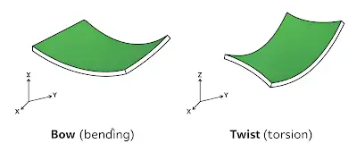
How unbalanced copper forces the panel to move during cool-down
The dominant driver we see every day is copper-area imbalance. Copper expands at roughly 17 ppm/°C while FR4 in the Z-direction runs 50–70 ppm and in the X-Y plane closer to 12–16 ppm. When one side of the stack carries 70 % copper and the opposite side only 30 %, the copper-rich side contracts harder during the cool-down from 180 °C lamination peak. Residual compressive stress builds on the copper-heavy face and the panel bows toward the copper-light face. Internal layers follow the same rule: a dense power plane opposite a sparse signal layer creates the same moment arm. We measure this risk by running a simple copper-percentage check layer by layer in the CAM system before releasing the job.
CTE mismatch alone is not enough; the stress is locked in by the resin flow and gelation that occurs under pressure. Once the resin crosses its glass-transition temperature and then cools under clamp pressure, the differential contraction becomes permanent. Rapid cool-down rates (common on older presses) freeze more stress; controlled ramp-down below 2 °C/min reduces it but never eliminates it if the copper is badly unbalanced.
Why thin cores and asymmetric stack-ups amplify the same stress
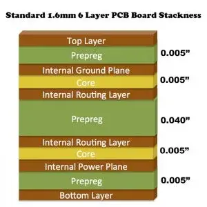
Board thickness and layer count change the stiffness. A 0.8 mm four-layer board has almost no bending resistance compared with a 2.0 mm eight-layer construction. The same copper imbalance that produces 0.4 % warpage on a thick board can easily reach 1.5 % on a thin one. Asymmetric stack-ups—core-heavy on one side, prepreg-heavy on the other—add another moment. We also see higher twist when the panel is routed with long unsupported edges or when the break-away tabs are placed only on two opposite sides; the free edges allow the residual stress to relieve itself into a helical shape.
What actually fails on the line when the numbers go out of limit
If the finished board leaves the factory with more than the allowed warpage or twist, the next problems appear at the customer's SMT line. Fine-pitch BGAs and QFNs refuse to sit flat; paste volume under the package becomes uneven and voiding or open joints follow. Wave-soldering fixtures no longer hold the board level, so components float or tombstone. In the worst cases the board rocks on the conveyor and the selective-soldering nozzle cannot maintain consistent height. On the fab side we also lose yield: panels that bow more than 1.5 mm over 300 mm length jam in the automatic optical inspection or electrical-test fixtures, forcing manual handling and extra scrap. Shipping delay is common once we have to re-bake or re-panelize a lot.
CAM and process steps factories use to keep FR4 PCB warpage under control
First action is always copper balancing. We add non-functional copper thieving or solid copper fill on sparse layers so that the copper percentage of every pair stays within 10–15 %. For internal planes we prefer mesh copper rather than solid when the opposite layer is open; the mesh reduces the absolute copper volume while still providing thermal balance. Stack-up is forced to be as symmetric as the electrical design allows—same core type and prepreg count mirrored about the centerline.
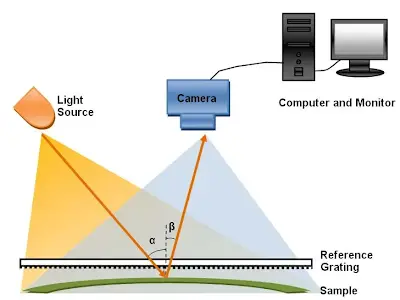
On the press side we run a slow cool-down profile after the high-pressure hold: from peak temperature down to 100 °C at ≤1.5 °C/min, then free cool. After depanelization every thin board (<1.0 mm) goes through a stress-relief bake at 150 °C for 2–4 hours under a flat aluminum plate with 5–10 kg distributed weight. Thick boards receive the same bake only if the first measurement already exceeds 0.5 %. Final measurement is done with a three-point or full-scan warpage tester per IPC-TM-650 2.4.22; any panel outside limit is re-baked once. A second failure ships only with customer waiver.
Panelization also helps. We keep the working panel size moderate (typically 18 × 24 in or smaller for thin material) and place solid copper borders or tooling strips that act as mechanical stiffeners. Routing tabs are distributed on all four sides so residual stress cannot relieve itself into a free twist.
Cases where the factory will accept a looser limit
When the board is thicker than 2.4 mm and carries only through-hole components, we sometimes relax the limit to 1.0 % because the stiffness itself prevents further movement at assembly. Prototype quantities under 20 pieces may ship with a simple flatness note if the customer confirms they will use vacuum fixtures. Rigid-flex sections are evaluated only on the rigid zones; the flex tails are allowed higher local deformation. In all these cases the trade-off is clear: higher risk of secondary warpage after reflow, so the customer must own the assembly process control.
From the fabrication side the message is consistent—copper balance and symmetric construction remove most of the stress before it ever forms. Once the residual stress is locked in, the only remaining tools are controlled cooling, weighted baking, and careful panel design. Designers who keep the copper-area difference under 15 % and avoid single-sided dense planes rarely see FR4 PCB warpage or twist become a production issue.






