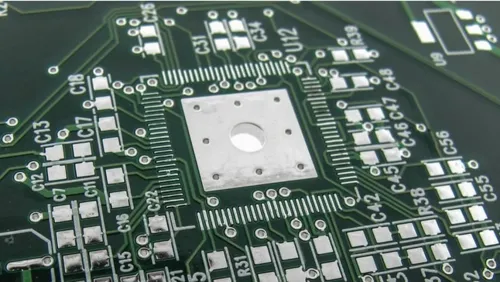
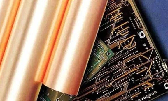
In production we treat insufficient HDI copper pour clearance as a hard stop at CAM review. When a pour comes closer to a microvia pad, trace, or SMD pad than the etch process can hold, the job is either pulled back in clearance or the copper region is isolated. On most HDI lines running 0.5 oz outer foil we enforce a finished copper-to-copper gap of 3.5 mil minimum after etch compensation; inner layers usually sit at 4–5 mil once the process factor is added. Designs that land below that number get flagged and corrected before the film or laser data is released.
Why sequential build-up and etch undercut make HDI copper pour clearance so sensitive
HDI sequential lamination is the root cause. Each laser microvia layer and each lamination cycle adds 1–2 mil of registration shift between the copper foil and the underlying features. A pour that looks clean against a via pad in the Gerber file often ends up with a local neck or bridge once the material has moved and the etchant has undercut the copper. Outer-layer 0.5 oz foil typically sees 0.3–0.5 mil undercut per side; on thinner 1/4 oz foils the undercut percentage is higher relative to the remaining conductor width. When the designer has already pushed the pour to 3 mil or less, that undercut plus the registration stack-up leaves almost no margin.
Local copper density makes the problem worse. Large pour areas next to dense via fields etch slower than isolated traces because the copper load changes the local etch rate. The pour edge therefore advances unevenly, closing the gap in the densest zones first. We see this repeatedly on boards with solid ground pours surrounding BGA microvia arrays—exactly the places where HDI copper pour clearance is most critical and most often violated.
What actually fails on the floor when the clearance is left too tight
Once the etch is finished, AOI or electrical test finds the bridges. The most common failure is an intermittent short between the pour and a microvia pad or an adjacent signal trace. On isolation test the board fails; on continuity the short may be solid or only appear after thermal stress. In the worst panels the entire lot is scrapped because the bridges are too widespread to rework by hand. Even when only a few nets are affected, the boards still have to be sorted, the good ones re-tested, and the schedule slips by at least one day—sometimes more if the panel has to be remade.
Assembly downstream feels the problem too. A pour that has partially shorted to a via pad can survive electrical test if the contact is marginal, then open or create leakage after reflow. That turns into field returns that are almost impossible to attribute correctly without cross-sectioning. From the factory side, every one of those returns traces back to an HDI copper pour clearance that was left inside the process capability limit.
How CAM and process actually recover the clearance before the panel runs
The first action is a clearance check against the process table for that copper weight and layer type. Any pour-to-feature gap below the finished requirement is either expanded by moving the pour edge or isolated by deleting the offending copper segment. We apply a positive etch compensation of 0.3–0.5 mil per side on outer layers and slightly more on inner layers so that the final conductor width and spacing land inside the design intent. That compensation is locked into the CAM data before laser drill or photo-tool generation.
On the panel side we also look at copper balance. Large solid pours next to sparse areas create differential etch rates that can close local clearances even when the nominal gap is acceptable. When that imbalance shows up we add dummy copper or split the pour into smaller regions with deliberate isolation channels. The isolation channels themselves are drawn at the same minimum clearance so they do not introduce new tight spots.
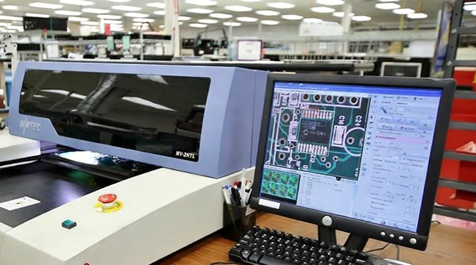
Final verification uses AOI with a tighter isolation threshold for pour regions. Any residual bridge that still appears after etch is either accepted under a documented deviation or the panel is rejected. The entire sequence—clearance check, compensation, balance adjustment, AOI—keeps the HDI copper pour clearance inside the process window without requiring the designer to resubmit the board.
When the factory can accept a tighter HDI copper pour clearance
We relax the rule only under three conditions that are written into the traveler. First, the copper must be 1/4 oz or thinner so the undercut percentage is smaller in absolute terms. Second, the nets involved must be low-voltage or non-critical so a marginal short does not create a functional failure. Third, the customer must accept the yield risk and the extra AOI or micro-section cost. Even then the exception is logged, the panel is run on a slower etch recipe, and the price is adjusted. Outside those conditions the clearance stays at the process minimum—no exceptions for schedule or volume.
Designers who keep the HDI copper pour clearance at or above the finished 3.5 mil outer / 4–5 mil inner numbers almost never see this issue reach the CAM desk. The ones who push below it create the exact sequence of registration shift, etch undercut, and local bridging that the factory has to clean up every time.