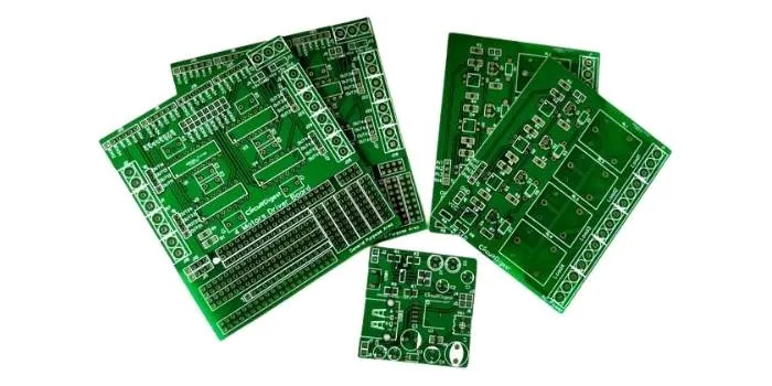
In production we price a 4-layer board from the panel yield first. CAM looks at the finished board outline against our standard 18" × 24" or 20" × 24" panels, subtracts the border, tooling holes and routing channels, then calculates how many units fit. That utilization number sets the base material cost before any copper weight, stackup or surface finish is added. Copper thickness, dielectric grade, via structure and order quantity then layer on top of that panel cost. The 4 layer pcb manufacturing cost moves most when any one of those items forces a non-standard process step or drops panel efficiency below about 75 %.
Where panel size and board thickness start driving material consumption
A 100 mm × 80 mm board usually nests cleanly and leaves room for rails and coupons. Drop the outline to 150 mm × 200 mm and the same panel may hold only two or three units once you keep the minimum 5–7 mm edge clearance for clamping and the 2 mm routing path between boards. Thicker cores (1.6 mm finished instead of 1.0 mm) also raise the laminate cost per square meter and reduce the number of panels that fit in a press cycle. We see the unit price jump 15–25 % on those larger or thicker boards purely from material waste and lower press throughput, even before copper or finish is considered.

How copper weight and laminate grade change etch and press time
Standard 1 oz outer copper on FR-4 Tg 135 is the baseline we quote most often. Moving to 2 oz outer copper lengthens the etch cycle and increases undercut compensation, so CAM adds extra spacing rules and the plating line runs longer. High-Tg or low-loss materials (Tg 170 or halogen-free) cost more per sheet and often require a different press recipe or slower heat-up rate. In the shop those changes show up as fewer panels per shift and higher scrap when the material is not already staged for the job. The 4 layer PCB manufacturing cost therefore carries a clear adder once copper exceeds 1 oz or the dielectric leaves the standard FR-4 family.
Stackup and impedance control that force extra lamination steps
A symmetrical 4-layer stack with 2116 prepreg and 1.6 mm finished thickness is routine. When the design calls for controlled impedance on both outer and inner layers, or mixes different prepreg styles to hit a target dielectric constant, the CAM engineer has to lock the stackup and the press cycle becomes job-specific. Registration tolerance tightens because the thicker or mixed dielectric expands differently; we typically allow ±75 µm layer-to-layer instead of the normal ±100 µm. Those boards sit longer in the press queue and need extra coupons for impedance verification, both of which raise the process cost.

Via and drill requirements that add machine time and defect exposure
Mechanical through-holes at 0.3 mm finished diameter are standard and run on the same drill machines as the rest of the job. Drop below 0.25 mm or add buried vias between layers 1–2 and 3–4 and we switch to a smaller bit, slower feed rate, and a separate plating cycle for the buried structures. Each extra drill hit and the additional desmear/plating steps consume capacity on the high-aspect-ratio lines. Yield also drops a few points because the smaller holes are more sensitive to resin smear and plating voids. Factories therefore load a noticeable cost adder once the via strategy leaves plain through-hole.

Surface finish and mask choices that insert extra process stations
HASL is still the lowest-cost finish because the panels already travel through the solder pot as part of normal flow. ENIG, immersion silver or OSP each require a dedicated chemical line, additional rinse cycles and tighter handling to avoid oxidation. White or black solder mask, or a requirement for 50 µm mask thickness instead of the usual 20–30 µm, also slows the coating and curing stations. These options do not change the panel yield, but they occupy equipment that could otherwise run standard jobs, so the factory books them as process adders on the 4 layer pcb manufacturing cost.
Setup cost behavior when quantity drops or lead time compresses
A prototype order of 5–10 panels carries the full CAM setup, first-article verification and machine changeover. Those fixed hours are spread across very few boards, so the unit price stays high. At 50–100 panels the same setup is amortized and the incremental cost falls to material plus direct labor. Quick-turn requests (3–5 days) force the job ahead of the normal queue, which means overtime on the drill and press lines and sometimes partial-panel runs that waste material. We therefore quote a separate expedite factor rather than simply scaling the standard volume price.
How the factory keeps 4-layer cost inside normal bounds
CAM first maximizes panel utilization by rotating boards, adjusting rail widths to the minimum that still allows clamping, and adding only the coupons required for the process. We hold copper to 1 oz outer / 0.5 oz inner unless the current density demands more, and we stay with standard FR-4 Tg 135 and a symmetrical stack whenever impedance can be met inside that window. Through-hole vias are preferred; buried or microvia structures are quoted separately and only after the designer confirms the layer assignment. Surface finish stays HASL or ENIG unless a specific soldering or shelf-life requirement forces the change. For volume orders we lock the stackup and material early so the press can run continuous batches instead of single-job recipes. These steps keep the majority of 4-layer jobs on the standard cost curve.
When the factory accepts a higher-cost configuration
High-speed designs that truly need low-loss dielectric or 2 oz copper on the signal layers are accepted, but the quote includes the material premium and the reduced press throughput. Prototype quantities under 20 panels are also run without forcing panel optimization, because the setup cost already dominates. In both cases the customer is told the exact adder and the yield expectation so the decision stays on the design side rather than appearing as an unexpected factory charge later.
Conclusion
In production the biggest swings in 4-layer PCB manufacturing cost still come from panel utilization and non-standard process steps rather than from the board size alone. Once copper stays at 1 oz, the stackup stays symmetrical FR-4, vias stay mechanical through-hole, and the quantity reaches a few dozen panels, the unit price settles close to the standard curve. Anything that forces a special press recipe, extra plating cycle, or poor nesting is what moves the quote. CAM flags those items early so the designer can decide whether the electrical requirement justifies the adder before the job is released.
FAQ
Q1: Does adding test coupons raise the 4-layer board cost?
A1: Yes, when the coupons consume panel space that could have held finished boards. Impedance or thermal-stress coupons are placed in the border or between units. If they force the array down by one board, material cost per unit rises. Most factories keep coupons to the minimum required by the process and quote the difference only when the customer asks for extra verification pieces.
Q2: How does solder-mask color affect pricing on a 4-layer job?
A2: Green is the default and runs on the standard coating line. White, black, or blue usually need a separate ink and longer cure time, so the panels occupy the mask station longer. The adder is small on volume runs but becomes visible on prototype quantities where machine changeover is not amortized. Factories treat non-green mask as a process option rather than a material change.
Q3: Is there a cost difference between 1.0 mm and 1.6 mm finished thickness when everything else is the same?
A3: 1.6 mm uses more laminate per panel and slightly reduces the number of panels that fit in a single press load. The material difference is straightforward; the throughput difference appears only when the press is already capacity-constrained. For most standard FR-4 jobs the price gap stays modest unless the thicker board also forces a change in prepreg style or copper weight.
Q4: Do factories charge extra for tight impedance tolerance on a normal 4-layer stackup?
A4: When the tolerance is tighter than ±10% and the stackup is still standard FR-4, the main cost is the extra coupons and the time spent measuring them, not a change in material or press. If the tolerance cannot be met without switching prepreg or dielectric grade, then the material and process adders apply. CAM usually confirms the achievable tolerance with the standard stack before quoting a special material.
Q5: What happens to cost if the design needs both ENIG and selective hard gold?
A5: Selective hard gold requires an extra plating step and a plating-resist pattern that is not used for standard ENIG. The panels go through an additional process station and the yield risk on the gold fingers is higher. Factories quote this as a dual-finish option with a clear process adder; it is not treated as a simple surface-finish upgrade.