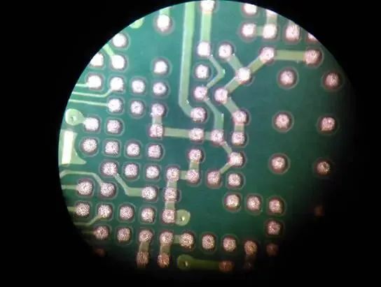
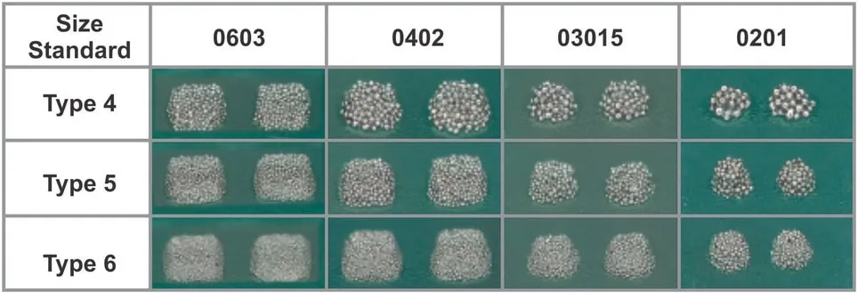
On an SMT production line, there is a saying: printing accounts for 70% of success, placement the remaining 30%. Solder paste printing quality largely determines final PCBA yield. The tooling at the heart of that 70% is the solder paste stencil. To align design and manufacturing practices, IPC published IPC-7525B, the industry's reference guide for stencil design.
What IPC-7525 Covers
IPC-7525 provides unified guidance for the design and fabrication of stencils used with solder paste and SMT adhesives. It is a design guide rather than a mandatory rulebook because printing performance depends on many variables (paste rheology, squeegee pressure, separation speed, aperture wall quality, and more). Still, it distills practical experience from global electronics manufacturers and serves as a reliable map to avoid process pitfalls.
Five Core Terms You Must Know
- Aperture: An opening in the stencil through which solder paste is printed onto the PCB pad.
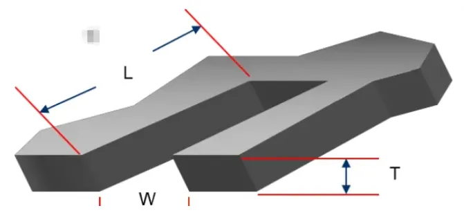
- Area ratio: The ratio of the aperture opening area (bottom area) to the aperture wall area. This is the key indicator of whether paste will release cleanly from the stencil.
- Aspect ratio: The ratio of aperture width to stencil thickness.
- Overprint (aperture oversize): An aperture intentionally larger than the PCB pad to increase deposited paste volume or improve coverage.
- Step stencil: A stencil with locally varied thickness to deliver different paste volumes for different component types on the same PCB.
Step One: Data Exchange and Preparation
Even the best stencil shop cannot produce a good stencil without accurate data. IPC-7525 defines expectations for data delivery:
- Preferred format: Gerber RS-274X is recommended because it contains all aperture information. If RS-274D is used, include a complete D-code table (aperture list).
- Supplementary layers: In addition to the paste mask layer, provide the solder mask, silkscreen, and, if possible, copper layers. These help the stencil supplier anticipate keep-out regions and optimize aperture shapes and clearances.
- Panelization and identification: For panelized builds, specify panel orientation and spacing. Each stencil should be clearly marked with an identifier, revision, thickness, and fabrication date to support traceability in production.
Core Rules: The Golden Principles of Aperture Design
Aperture design directly determines print quality. The following rules capture the essential physics and practical adjustments that drive robust printing.
1. Paste Release Physics: Area Ratio and Aspect Ratio
Paste release is fundamentally a competition of adhesion: the paste must prefer the pad over the aperture walls. Two geometric metrics control that outcome:
- General threshold: Aspect ratio > 1.5 and area ratio > 0.66 are widely accepted as robust minimums for reliable release.
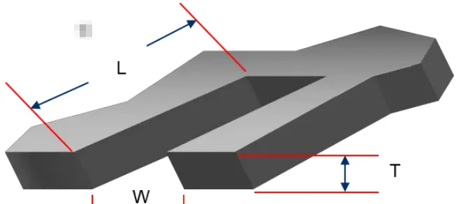
- Advanced capability: With modern processes such as laser cutting followed by electropolishing, precision electroforming, and other treatments that produce extremely smooth aperture walls, reliable release can be achieved at area ratios down to about 0.5, depending on paste and process conditions.
2. Lead-Free vs. Sn-Pb: Different Aperture Strategies
Wetting characteristics differ between lead-free and Sn-Pb pastes, driving different aperture choices:
- Lead-free paste: Lead-free tends to wet less aggressively. To ensure adequate coverage after reflow, match aperture size to pad size as closely as possible (approximately 1:1). If needed, reduce width slightly—on the order of about 0.0127 mm per side. For BGAs and fine-pitch parts, consider overprint (aperture larger than pad) to ensure sufficient paste volume.
- Sn-Pb paste: Sn-Pb wets readily and can spread more. To prevent bridging and solder balling, modestly reduce apertures. For gull-wing leaded packages, typical reductions are approximately 0.03–0.08 mm in width and 0.05–0.13 mm in length.
3. Component-Specific Guidelines
| Component type | Key aperture design points | Mistake-proofing tips |
|---|---|---|
| Fine-pitch QFP | Tightly control area ratio to avoid clogging. | Reduce width slightly to maintain spacing and reduce bridging risk. |
| BGA / CSP | For molded BGAs, mitigate head-in-pillow by ensuring adequate paste volume. | Square apertures can improve release versus round for the same pad size. |
| Chip resistors/capacitors | Prevent excess paste under the body that can cause tombstoning or solder balls. | Use recessed "U" shapes, hourglass (dumbbell) cuts, or small circular reliefs on the pad ends. |
| BTC/LCC thermal or ground pads | Thermal/ground pads printed as a full aperture can wick excessive solder and tilt the component. | Windowpane the aperture, reducing effective area by about 20–50%. |
If a pad contains vias, avoid them with the stencil aperture to prevent solder wicking and insufficient joints.
Designing for Special Process Scenarios
As product complexity increases, a flat, single-thickness stencil may not satisfy all requirements. IPC-7525 addresses several special situations.
1. Adhesive Printing Stencils (SMT Glue)
SMT adhesive typically has much lower viscosity than solder paste and can easily bleed under the stencil. To maintain board contact and prevent bleed-out, adhesive stencils often require relieved features on the board side—such as step-etched clearance pockets—to bypass labels, silkscreen, or raised plating that would otherwise interfere with gasketing.
2. Pin-in-Paste (PIH) for Through-Hole Reflow
Combining SMT and THT in a single reflow pass hinges on stencil design. Through-hole reflow requires large paste volumes, and the calculation depends on hole diameter, pin diameter, board thickness, and other variables.
- Practical approach: Use a step stencil that locally increases thickness in the PIH region (often to 0.2 mm or even 0.3 mm or more) and significantly overprint the aperture (commonly to an effective size on the order of 4–6 mm relative to the hole) to achieve full hole fill after reflow.
3. Step Stencils
Many assemblies mix ultra-small passives (e.g., 03015) with large connectors, demanding very different paste volumes. A step stencil can balance these requirements:
- Step-down: Reduce thickness on the squeegee side to decrease paste volume, used for larger components when less paste is desired.
- Step-up: Reduce thickness on the PCB contact side to increase effective paste transfer for dense-pitch regions where more volume is needed.
- Local relief: Add localized recesses to clear tall components on the opposite side of the PCB, maintaining good gasketing.
Manufacturing, Acceptance, and Maintenance
A robust design must be supported by capable fabrication, verification, and upkeep.
- Stencil fabrication methods:
- Chemical etch: Lower cost, but tapered/rough walls. Suitable for larger pitch work.
- Laser cut with electropolish: Mainstream choice. Vertical, smooth walls and high dimensional accuracy.
- Electroformed: Extremely smooth walls and superior release; favored for very fine pitch (e.g., 0.3 mm QFP, 0.4 mm BGA).
- Incoming inspection (IQC): Verify stencil tension (often specified as greater than 30 N/cm2), aperture dimensional accuracy, and burr condition before use.
- Cleaning and service life: Stencils are consumables. Follow cleaning and maintenance practices in IPC-7526, using appropriate equipment and solvents at defined intervals. If apertures deform, walls are scratched, or tension degrades beyond limits, retire the stencil.
Closing Thoughts: Precision and Discipline Drive Yield
IPC-7525 is more than a technical document; it reflects the industry's commitment to precision and standardization. With DFM increasingly integrated into development, having process engineers influence stencil aperture design early—grounded in IPC guidance—has become standard practice for improving yields and controlling cost. When aperture geometry, stencil fabrication, printing parameters, and paste properties are treated as a coherent system, print performance becomes stable and predictable.