Objective
To increase solder deposition relative to the current design, a 0.25 mm square aperture with corner radius R = 0.05 mm was selected for verification. SPI was used to measure and compare printed height, area, and calculated volume, and to compute CPK. Downstream electrical test and assembly data were then used to assess the feasibility of the proposed aperture.
Experimental Plan
Based on theoretical geometry, the 0.25 mm rounded-square aperture offers a larger paste area than the 0.26 mm round aperture, which is favorable for increasing solder volume. The area ratio (AR) of the two designs is comparable. The theoretical paste volume increase of the rounded-square aperture is approximately 13.6% versus the 0.26 mm round. Release (de-molding) behavior and bridging risk were to be verified in production.
The left image below shows the 0.25 mm rounded-square aperture (R = 0.05 mm) and the right shows the 0.26 mm round aperture. The BGA ball pitch is 0.4 mm center-to-center.
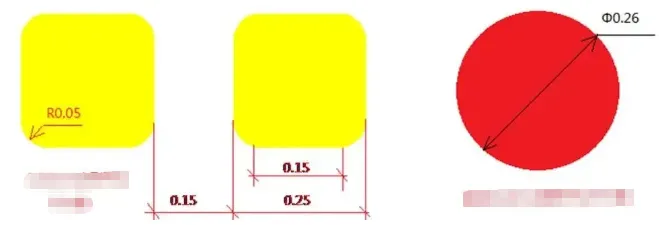
Figure | Aperture geometry and dimensions: 0.25 mm rounded-square (R = 0.05 mm) versus 0.26 mm round for a 0.4 mm-pitch BGA.
Validation Plan
4.1 The validation was executed on a mass-production project, with the main chip MSM8909. Stencils were prepared per the above aperture definitions.
4.2 During SMT placement of the project, the 0.25 mm rounded-square stencil and the 0.26 mm round stencil were alternated. Post-print SPI inspection confirmed print quality, and CPK was calculated. Reflowed assemblies were tracked through downstream test data.
Data Collection Plan
4.3.1 Confirm post-print condition and collect SPI data for each aperture. Calculate solder paste height, area, and volume CPK, as well as printed volume.
4.3.2 Collect data continuously in sequence to maintain measurement continuity.
4.3.3 Record barcode ranges for boards printed with the 0.25 mm rounded-square stencil for traceability in downstream analysis.
4.3.4 Correlate downstream test data, and examine main-chip failures to determine whether they originate from SMT.
4.3.5 Review distribution of bridging and opens, if any.
4.3.6 Based on the statistics, determine the aperture with higher solderability and continue validation in subsequent products.
Validation Procedure
5.1 Equipment: SPI inspection system KY8030-2 (KOH YOUNG TECHNOLOGY).
5.2 Execution: On May 17, 2016, the project ran in mass production using the baseline 0.26 mm round CPU stencil. A sample of 60 pcs was extracted for SPI testing. During the same build, the stencil was switched to the 0.25 mm rounded-square design, and 60 pcs were printed. With 504 BGA pads per board, the total number of BGA paste deposits inspected was 60 × 504 = 30,240. SPI data were recorded for analysis.
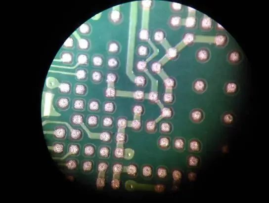
5.4 Post-print microscopic inspection indicated acceptable print quality for both apertures.
Post-print photos—0.25 mm rounded-square aperture:
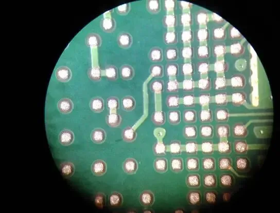
Figure | Post-print deposits with 0.25 mm rounded-square apertures.
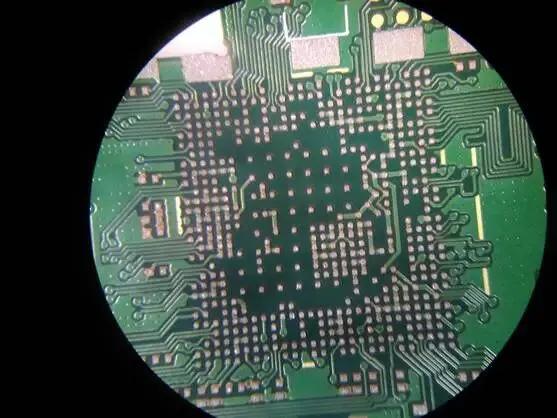
Figure | Additional view of 0.25 mm rounded-square post-print deposits.
Post-print photos—0.26 mm round aperture:
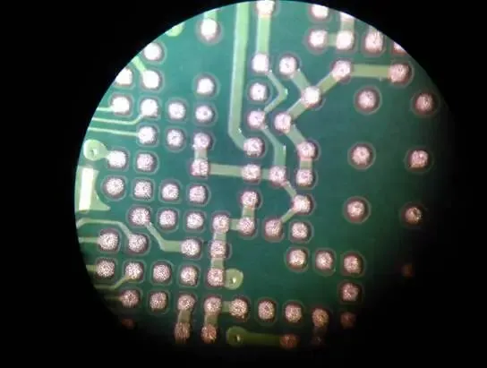
Figure | Post-print deposits with 0.26 mm round apertures.
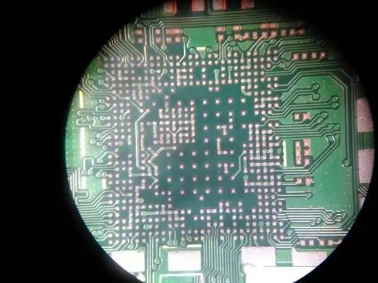
Figure | Additional view of 0.26 mm round post-print deposits.
SPI Inspection and Statistics
Unless otherwise specified, stencil thickness was 0.10 mm for both apertures, printed on the same printer with identical process parameters.
Height limits: (stencil thickness ? 0.03) to (stencil thickness + 0.03). Area limits: aperture area ±30%. These limits reflect common industry practice and internal OEM guidelines.
0.25 mm rounded-square aperture results:
5.5.1 Height (HEIGHT) average = 93.1345.
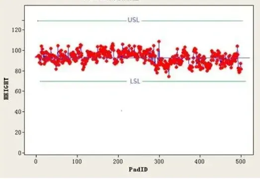
Figure | Height scatter for 0.25 mm rounded-square prints.
5.5.1 Area (AREA) average = 92.9261% of the nominal stencil aperture area.
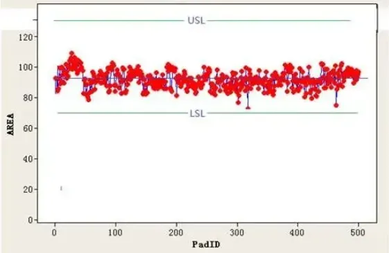
Figure | Area scatter for 0.25 mm rounded-square prints.
0.26 mm round aperture results:
5.5.2 Height (HEIGHT) average = 85.2583.
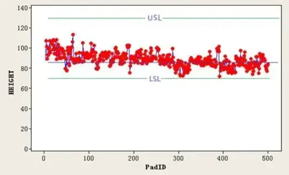
Figure | Height scatter for 0.26 mm round prints.
5.5.2 Area (AREA) average = 92.3079% of the nominal stencil aperture area.
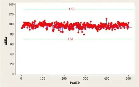
Figure | Area scatter for 0.26 mm round prints.
Data Analysis
6.1 Printing Height
The solder paste height CPK values for both apertures exceeded 2.5, with very small differences. Both stencils exhibited highly stable printing height and few paste "tails." The average paste height for the 0.25 mm rounded-square aperture was 93.1345, versus 85.2583 for the 0.26 mm round. With identical stencil thickness (0.10 mm) and identical printer settings, the slightly higher height observed for the rounded-square aperture is likely due to more difficult release at the aperture corners—minor edge pull-up can increase measured height.
6.2 Printing Area and Volume
Area CPK values for both apertures were above 2.4, indicating very stable area printability with clean release and minimal residual paste in the apertures. The measured average printed areas were:
- 0.25 mm rounded-square: 92.9261% × 0.06035 = 0.05608 mm2
- 0.26 mm round: 92.3079% × 0.05310 = 0.04902 mm2
These results align with the theoretical calculation that the 0.25 mm rounded-square design prints a larger area than the 0.26 mm round, and therefore delivers higher volume (volume ≈ area × stencil thickness). The rounded-square CPK was slightly lower than the round, likely because the rounded-square corners extend closer to the solder mask dam in some pad layouts; the mask is lower than the pad copper, leaving a small gap to the stencil that adds variability at the corners.
Overall, the 0.25 mm rounded-square aperture provides higher average height and area than the 0.26 mm round. Although its area CPK is slightly lower, both designs exceed CPK = 2.0 (excellent). To increase solder volume and reduce opens, the 0.25 mm rounded-square is preferred.
X-ray Inspection After Reflow
7.1 100% X-ray inspection was performed on all 30,240 BGA joints; no bridging was observed.
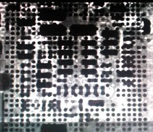
Figure | Representative X-ray image—no bridging detected.
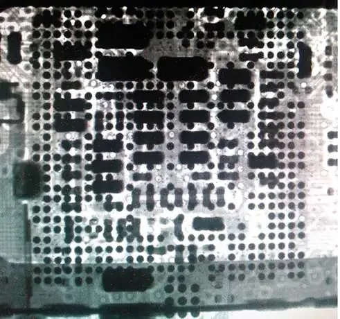
Figure | Additional X-ray image—uniform joints, no shorts.
7.2 Solder Ball Diameter Measurements
7.2.1 Measurement method: Using the 0.4 mm ball pitch as a reference, five-ball spacing equals 5 × 0.4 = 2.0 mm. With an on-screen caliper reading of 122.06 for five-pitch distance, the scale factor is 2 / 122.06. A measured on-screen ball diameter of 17.37 corresponds to D = 17.37 × 2 / 122.06 = 0.2877 mm.
7.2.2 For each group, ten balls were measured and averaged.
7.2.3 Analysis: The average solder ball diameter with the 0.25 mm rounded-square aperture was D1 = 0.2783 mm, and with the 0.26 mm round aperture was D2 = 0.2718 mm. The difference (~0.0065 mm) is small and can be neglected. The minimum clearance between adjacent balls satisfied the 0.10 mm safety requirement.
Downstream Test and Assembly Results
8. Test-stage failures: none observed.
9. Assembly-stage failures: none observed.
Conclusion
The 0.25 mm rounded-square stencil aperture (R = 0.05 mm) increased solder paste volume and demonstrated stable printability without bridging. Comprehensive performance was favorable. This aperture can be introduced in small-batch NPI and further validated for broader production deployment, with continued monitoring of mass-production data.
CPK Ranges and Process Capability Interpretation
- CPK < 0.67: Grade D, unacceptable; redesign or new process required.
- 0.67 < CPK < 1.00: Grade C, high defect risk; improvement needed.
- 1.00 < CPK < 1.33: Grade B, marginal; process drift can induce defects.
- 1.33 < CPK < 1.67: Grade A, good capability; stable.
- 1.67 < CPK < 2.00: Grade A+, very good; maintain.
- CPK ≥ 2.00: Grade A++, excellent.