A single-layer aluminum-based PCB measuring 93.15 mm × 49.99 mm entered CAM review with a clear thermal-management purpose. The order specified 1.6 mm aluminum substrate, 1 oz copper, white solder mask, black silkscreen, lead-free HASL, and mechanical forming. Quantity was 15 pieces delivered as five sets. Minimum hole size appeared as 3.5 mm in the parameters, and the customer note simply requested IPC Class 2. On the surface the data package looked straightforward for an MCPCB. Yet the outline layer contained large circular features whose diameters did not match any entry in the drill file, while the silkscreen layer carried additional circles that could be misread as drill targets. These discrepancies created an immediate interpretation gap: the factory could not decide which geometry governed the finished contour and which features required drilling. Production could not proceed until the design intent behind the mismatched circles was clarified.
Aluminum Board Design Intent and Thermal Outline Features
The apparent design objective was a compact aluminum PCB ( #ALU-20260531-057 ) intended for heat dissipation. The single copper layer, white solder mask, and black silkscreen are typical for LED or power modules that rely on the aluminum base for thermal conductivity. Mechanical forming was specified, process edge was zero, and no panelization array was required beyond the five-set shipping format. Large circular openings on the outline layer could have been intended as mounting clearances, thermal cut-outs, or decorative features. However, their diameters did not align with the drill list, and no fabrication note explained whether those circles were to be routed, drilled, or ignored. The silkscreen layer added further ambiguity by placing circles near arrow markers that visually resembled drill targets. Without a consistent definition linking the outline geometry to the drill data, the manufacturing path for both contour and hole generation remained open to conflicting interpretations.
Outline Layer Circles Inconsistent with Drill File
During the initial data cross-check our CAM engineer compared the outline layer against the drill file. Several large circles appeared on the outline (mechanical) layer, yet their diameters did not correspond to any tool size listed in the drill data. The order parameters indicated a minimum hole of 3.5 mm, but the outline circles were visibly larger and lacked matching drill entries. On an aluminum substrate the distinction is critical: a circle drawn on the outline layer is normally treated as a contour feature to be routed, while a drill entry generates a plated or non-plated hole. When the two sources disagree, the factory cannot determine whether material should be removed by routing bit or by drill bit, nor whether the finished opening must meet hole-location or outline-tolerance criteria.
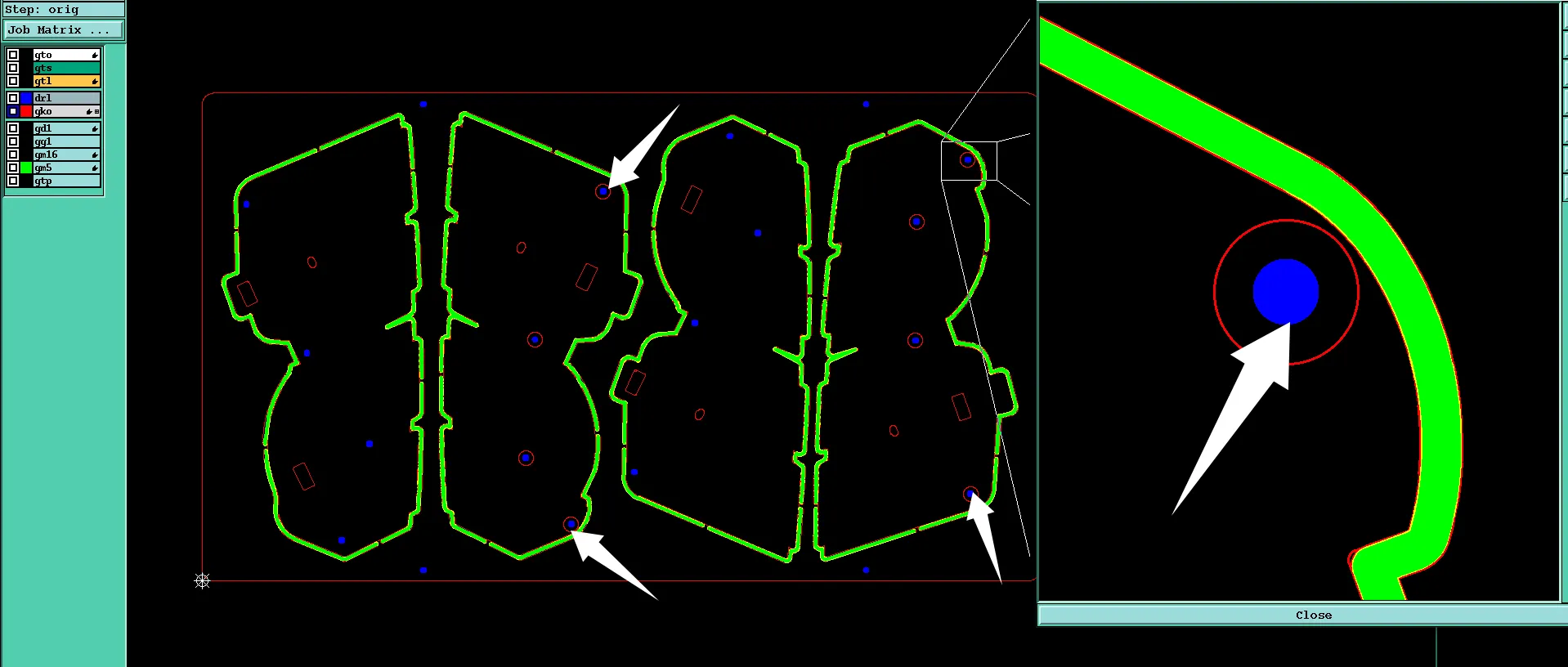
Figure 1: the drill size is different from the one in the outline
If the outline circles had been routed as drawn, the resulting openings would have exceeded the drill sizes and altered the thermal mass and mechanical strength of the aluminum base. If the drill file had been followed and the outline circles ignored, the finished board would retain material that the designer may have intended to remove. Either choice risked dimensional non-conformance under IPC Class 2 and potential thermal or mounting interference at assembly. The conflict therefore belonged to the data-to-data category: Gerber outline versus drill file, compounded by the absence of any explanatory fabrication note.
| Data Source | Feature Present | Diameter Match to Drill | Manufacturing Risk if Unresolved |
|---|---|---|---|
| Outline Layer | Large circles | No | Incorrect contour size or residual material |
| Drill File | Defined hole sizes | Reference | Missing openings if outline ignored |
| Fabrication Notes | None explaining circles | - | Ambiguous process path |
Silkscreen Circles Resembling Potential Drill Targets
A second observation reinforced the primary concern. On the character (silkscreen) layer, circles appeared at locations marked by arrows in the review notes. These circles had no corresponding drill entries and no electrical function. Because they were drawn with a diameter that could be mistaken for a small hole, the CAM system flagged them as possible undrilled features. On an aluminum PCB the risk is practical: if the factory drilled them, the aluminum base would receive unnecessary holes that reduce thermal mass and create potential leak paths for potting or conformal coating later. If the circles were left as silkscreen graphics, they would simply print as ink and cause no mechanical change. The ambiguity again prevented confident release.
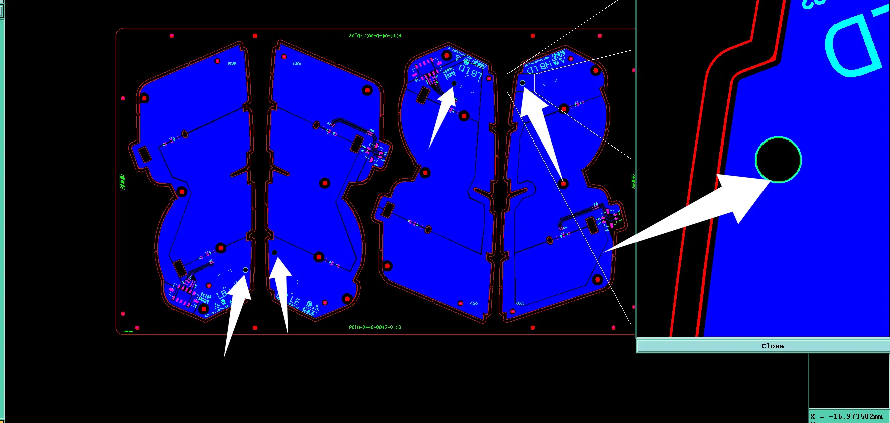
Figure 2: a circle at the arrow location on the character layer in the file
Both issues shared a common root: the design files contained circular geometry whose manufacturing treatment could not be deduced from the data alone. The outline circles conflicted with the drill file; the silkscreen circles lacked any drill definition. In the absence of clear notes, design intent remained open to multiple manufacturing interpretations.
Drill Priority Decision and Outline Circle Resolution
The engineering team treated the drill file as the authoritative source for all hole features and the outline layer as the source for external contour only. The large circles on the outline layer were therefore classified as non-drill geometry that should be ignored for drilling purposes. The customer was asked to confirm that the finished openings would follow the drill sizes and that the outline circles could be disregarded. Simultaneously the silkscreen circles at the arrow locations were identified as graphic elements only; they required no drilling and would be processed solely as part of the character layer.
Customer confirmation accepted both interpretations: follow the drill size and ignore the circles in the outline layer; treat the silkscreen circles as non-drill graphics. With the primary conflict closed, the CAM data were updated to suppress the outline circles from the routing path and to exclude the silkscreen circles from the drill list. The external contour remained defined by the true board outline, and all functional holes followed the verified drill file. The aluminum substrate therefore retained its intended thermal mass and mechanical integrity while still meeting the dimensional requirements of IPC Class 2.
| Engineering Observation | Conflict Identified | Recommended Action | Final Status |
|---|---|---|---|
| Large circles on outline layer | Diameter mismatch with drill file | Ignore outline circles; follow drill sizes | Confirmed |
| Circles on silkscreen at arrow locations | Possible misinterpretation as drill features | Process as graphics only; no drilling | Confirmed |
| No fabrication note explaining circles | Design-intent ambiguity | Customer clarification required | Received and applied |
Supporting Observations on Aluminum MCPCB Processing
Although secondary to the circle conflict, two additional points were noted because they interact with aluminum processing. The board carried zero process edge and relied on mechanical forming; any unintended material removal from misinterpreted circles would have reduced the effective thermal plane without recovery margin. Hole density was modest, yet the 3.5 mm minimum hole size already approached the practical limit for clean drilling in 1.6 mm aluminum without excessive burr. Confirming that only the drill-file entries would be drilled protected both edge quality and thermal performance. These observations did not generate independent holds once the primary drill-versus-outline decision was locked.
Final Engineering Release After Circle Clarification
With customer confirmation in hand, the outline layer was edited to suppress the non-matching circles from the contour path, the drill list remained unchanged, and the silkscreen circles were locked as graphic-only features. The CAM package was released for tooling. The finished aluminum boards followed the drill sizes for all openings, retained the intended external outline, and carried silkscreen graphics exactly as drawn. No further engineering questions arose, and the five-set order moved into production under the clarified design intent.
Design Lessons for Avoiding Drill-Outline Conflicts
- Any circle drawn on the outline layer must either match a drill entry or be explicitly noted as a non-drill contour feature; silent mismatches force CAM clarification.
- Silkscreen circles that resemble holes should be drawn with a line width or fill style that cannot be mistaken for drill targets, or a note should state they are graphics only.
- On aluminum PCBs the thermal mass is sensitive to every removed opening; unintended drilling or routing reduces heat-spreading capability without easy recovery.
- When drill file and outline layer disagree, the factory defaults to the drill file for holes and seeks confirmation before altering the contour.
- Zero process edge leaves no sacrificial material; any geometry change on the outline must be authorized before routing.
- IPC Class 2 still requires consistent hole location and outline accuracy; mismatched circles create dimensional risk even on simple single-layer aluminum boards.
- Provide a single fabrication note that states which layer governs hole generation and which layer governs external contour when circular features appear on both.
FAQ
Q1: Why does a large circle on the outline layer trigger an Engineering Question when the drill file already exists?
A1: The outline layer normally defines the board contour. When its circles do not match any drill size, the factory cannot decide whether to route the feature or ignore it. Confirmation prevents incorrect material removal.
Q2: Can silkscreen circles be drilled by mistake on an aluminum PCB?
A2: Yes. If the circles visually resemble drill targets and lack a clear “graphics only” note, automated CAM checks may flag them. Drilling them would create unnecessary holes that reduce thermal mass.
Q3: Why is the drill file given priority over the outline layer for hole features?
A3: The drill file is the explicit tool list. Outline circles without matching drill entries are treated as contour geometry unless the customer states otherwise.
Q4: What manufacturing risk exists if outline circles are routed on an MCPCB?
A4: The aluminum base loses thermal mass and mechanical strength in the removed areas. On a zero-process-edge board the dimensional change is permanent and may fail mounting or heat-spreading requirements.
Q5: How should designers prevent drill-versus-outline conflicts?
A5: Ensure every circular opening intended as a hole appears in the drill file with the correct diameter, and add a fabrication note for any outline circles that are purely contour features.
Q6: Does IPC Class 2 still apply when circles are mismatched on a simple aluminum board?
A6: Yes. Class 2 requires consistent hole location, diameter, and outline accuracy. Unresolved mismatches create dimensional non-conformance risk regardless of layer count.