


Engineering Cases
Engineering Cases focuses on real PCB engineering reviews, manufacturing challenges, and production optimization processes from actual fabrication projects. This category highlights how different PCB designs are evaluated and adjusted during engineering review, covering topics such as stack-up analysis, impedance control, drill optimization, copper balancing, solder mask alignment, DFM review, and production risk assessment across various PCB applications. The content in this section is based on practical manufacturing scenarios rather than theoretical introductions. Each engineering case demonstrates how specific PCB issues are identified, analyzed, and resolved during production preparation and fabrication. These records help engineers, purchasers, and hardware teams better understand the relationship between PCB design decisions and manufacturing stability, yield control, and process reliability. Topics may include multilayer PCB engineering review, HDI process optimization, flexible PCB manufacturing considerations, heavy copper processing adjustments, surface finish selection, Gerber data verification, and other real-world PCB production experiences. By organizing engineering challenges and process solutions into structured case content, this category provides valuable insight into practical PCB manufacturing and engineering workflow management.
Featured Blog
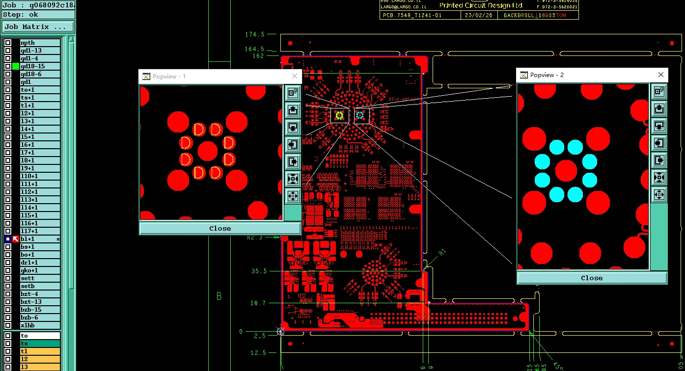
PCB Hole Attributes and Special Drilling: Common CAM Review Conflicts
See how CAM reads PCB hole attributes and special drilling—PTH vs NPTH, back drill, press-fit holes, countersink, and laser vias—and why incomplete data delays fabrication.
Latest Blogs
How Panelization Conflict Delayed Single Piece Delivery in 1-Layer PCB
Learn how mismatched panelization data and process edge requirements triggered an Engineering Question for a 1-layer FR4 PCB order. This CAM review case examines the investigation into V-CUT incompatibility, hole attributes, Gerber layer discrepancies, resolution through routing confirmation, and key lessons for designers to align data files with single piece delivery expectations for smooth manufacturing.
Resolving 12 layer FR4 PCB Copper Thickness and Impedance Conflicts
Explore how conflicting copper thickness specifications across stackup and impedance documents triggered a key Engineering Question during CAM review of a 12-layer FR4 PCB. This engineering case details the investigation into file format conflicts, via mask alignment, proposed stackup adjustments for impedance control, resolution process, and practical lessons for designers to ensure consistent documentation and manufacturable multilayer boards.
How DFM Review Secured Impedance Control in 6-Layer FR4 PCB
In this 6-layer FR4 project, DFM analysis identified critical risks including non-standard stackup, marginal trace widths for 90 ohm impedance, missing copper pour on L4 for 50 ohm control, and absent solder mask openings. Learn how proactive engineering adjustments ensured accurate impedance, reliable plating, and successful production, helping designers avoid common signal integrity and manufacturability issues.
Why Impedance Line Mismatches Triggered EQ in Multi-Layer PCB Production
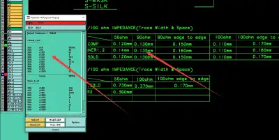
Discover how inconsistent impedance line identification between customer tables and production files triggered a critical Engineering Question during CAM review of a 8-layer FR4 PCB. This case details the engineering investigation, supporting mechanical concerns like stamp holes and silkscreen clearance, resolution process, and key lessons for designers to prevent similar data conflicts and ensure manufacturable impedance control.
Critical PCB DFM Review for Small Volume FR4 Production Runs
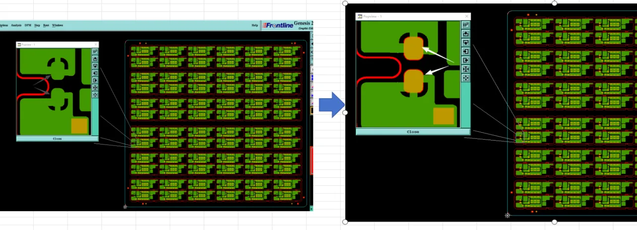
In a 5400-piece 2-layer FR4 order, DFM analysis uncovered tight stamp hole spacing, missing solder mask openings on pads, and challenging square slots that threatened panel integrity and yield. Learn how preventive engineering clarifications avoided breakage, ink coverage issues, and assembly failures, ensuring reliable high-volume production and long-term board quality.
How DFM Review Prevented Via Reliability Risks in a 2-Layer FR4 PCB
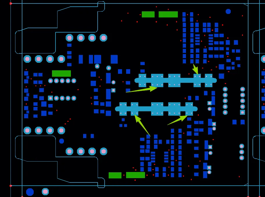
Discover how our DFM analysis identified critical via solder mask issues, plated slot conflicts, and dimensional discrepancies in a 2-layer FR4 working file. We explains the preventive actions taken to avoid ink intrusion, solder bead entrapment, and yield loss—ensuring reliable production and long-term PCB performance. Learn key lessons for better manufacturability.
Preventing Edge Breakout and Burr Risks in Aluminum PCB Panelization
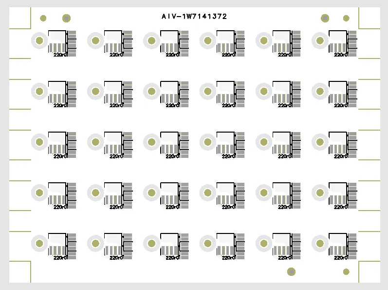
Explore how DFM review prevented edge breakout, burrs, and clearance issues in a single-layer aluminum PCB. Learn key manufacturability risks around countersink holes, V-cut panelization, and copper spacing to ensure high yield and thermal reliability before production.
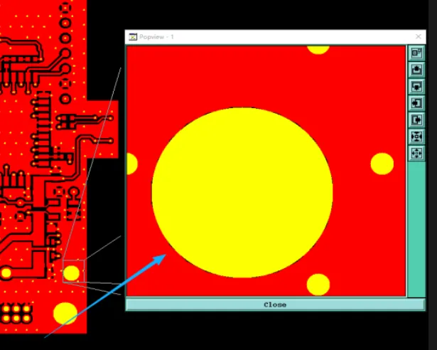
Preventing Exposed Copper and Via Plugging Risks in a Compact 4-Layer FR4 PCB
Discover how proactive DFM review prevented exposed copper, resin plugging inconsistencies, and impedance issues in a compact 4-layer FR4 PCB. Learn critical manufacturability risks and preventive strategies to protect yield and reliability before production begins.
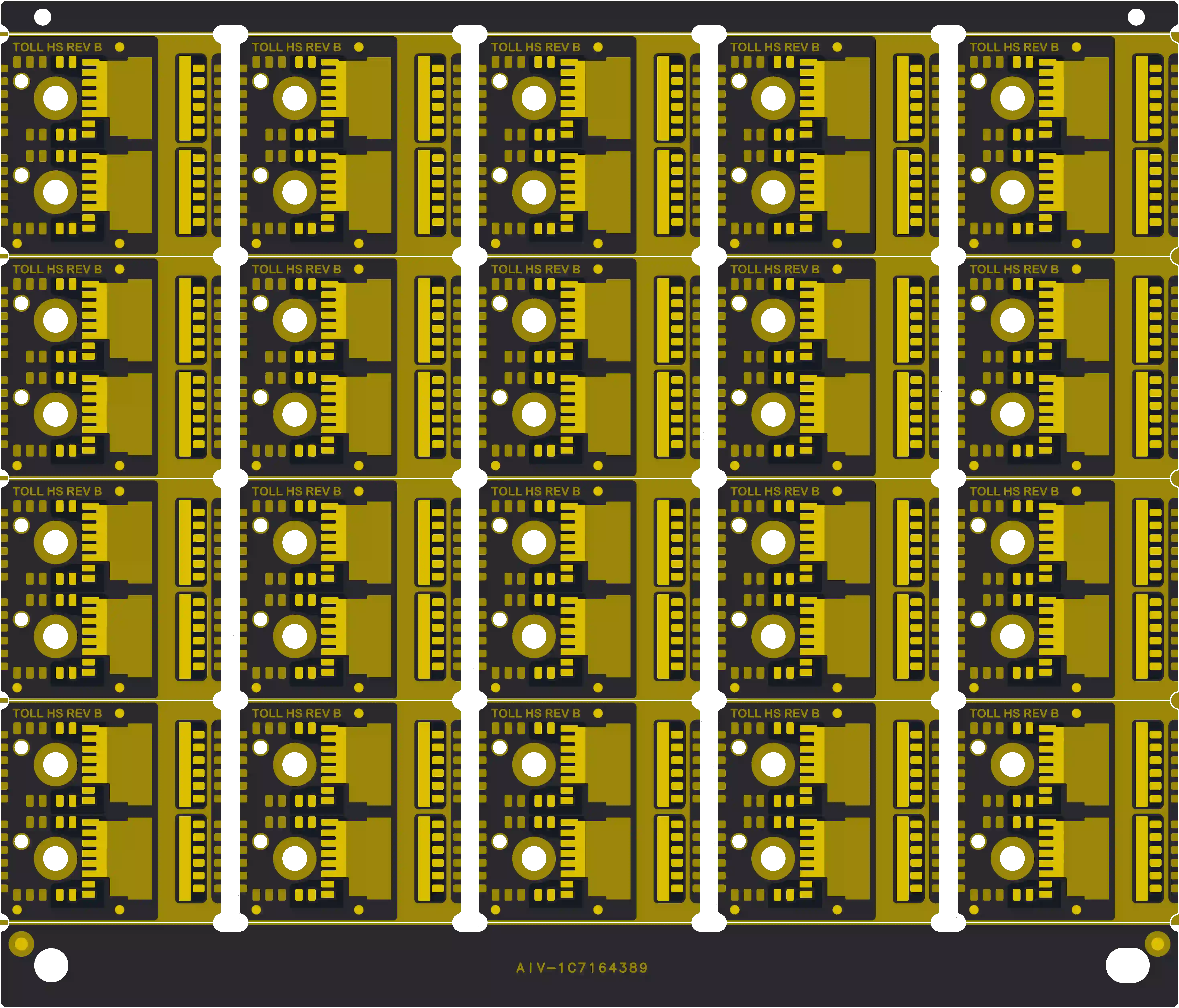
Stackup and Gold Thickness Limits in Thermoelectric Separation Copper Base PCBs
This technical assessment examines manufacturing capability for thermoelectric separation copper base PCBs. It focuses on the decision to adopt conventional stackup over customer documentation and the resulting 0.05µm ENIG gold thickness limit caused by direct connection between edge pads and base copper, while maintaining 380W thermal conductivity and insulation performance.
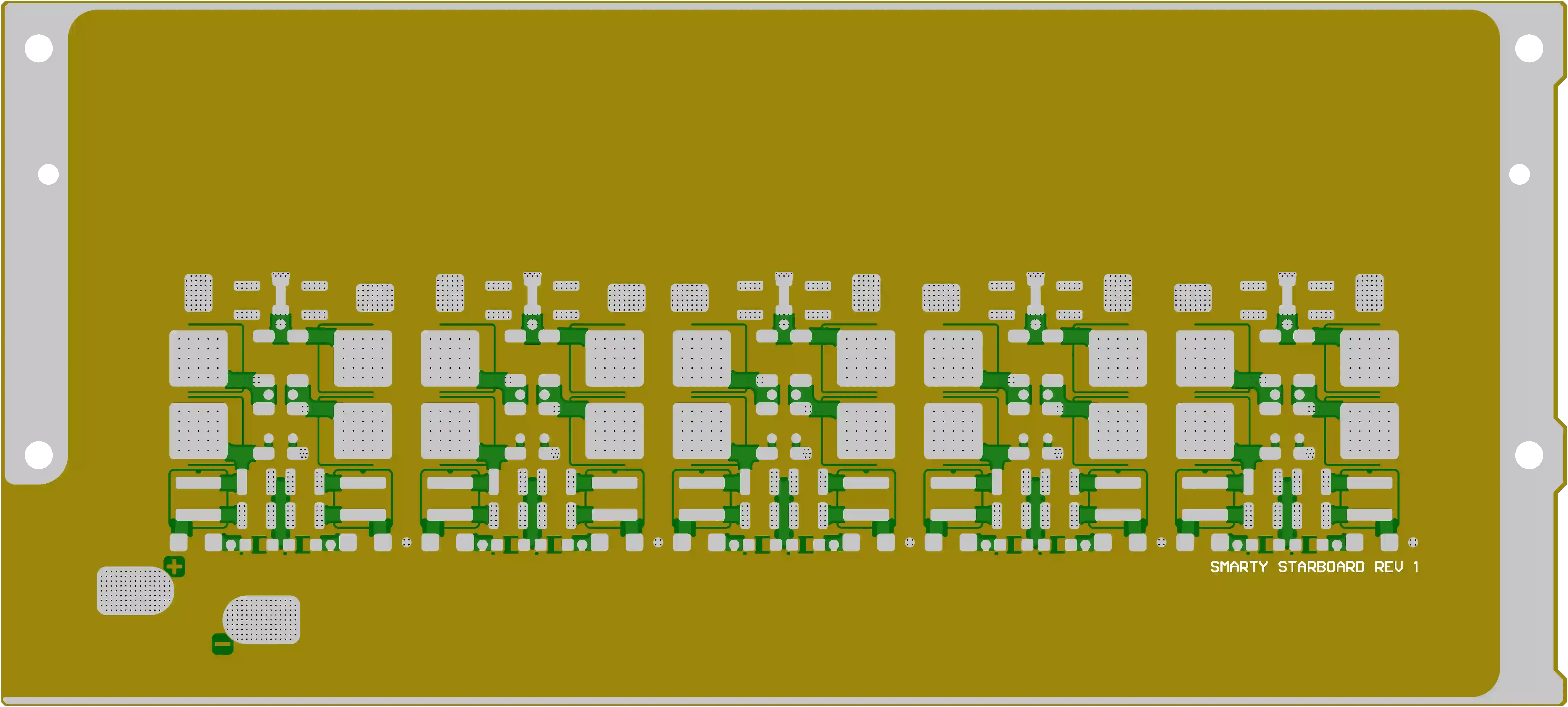
0.15mm Hole & Countersink Depth Control in 4-Layer HDI PCB
AIVON assesses manufacturing capability for a 4-layer FR4 PCB featuring 0.15mm holes, HDI blind vias, 1.6mm thickness, and 1.35mm countersink depth control. This technical review examines drilling precision limits, lamination adjustments, and process validation for reliable production of fine-feature boards with immersion silver finish.
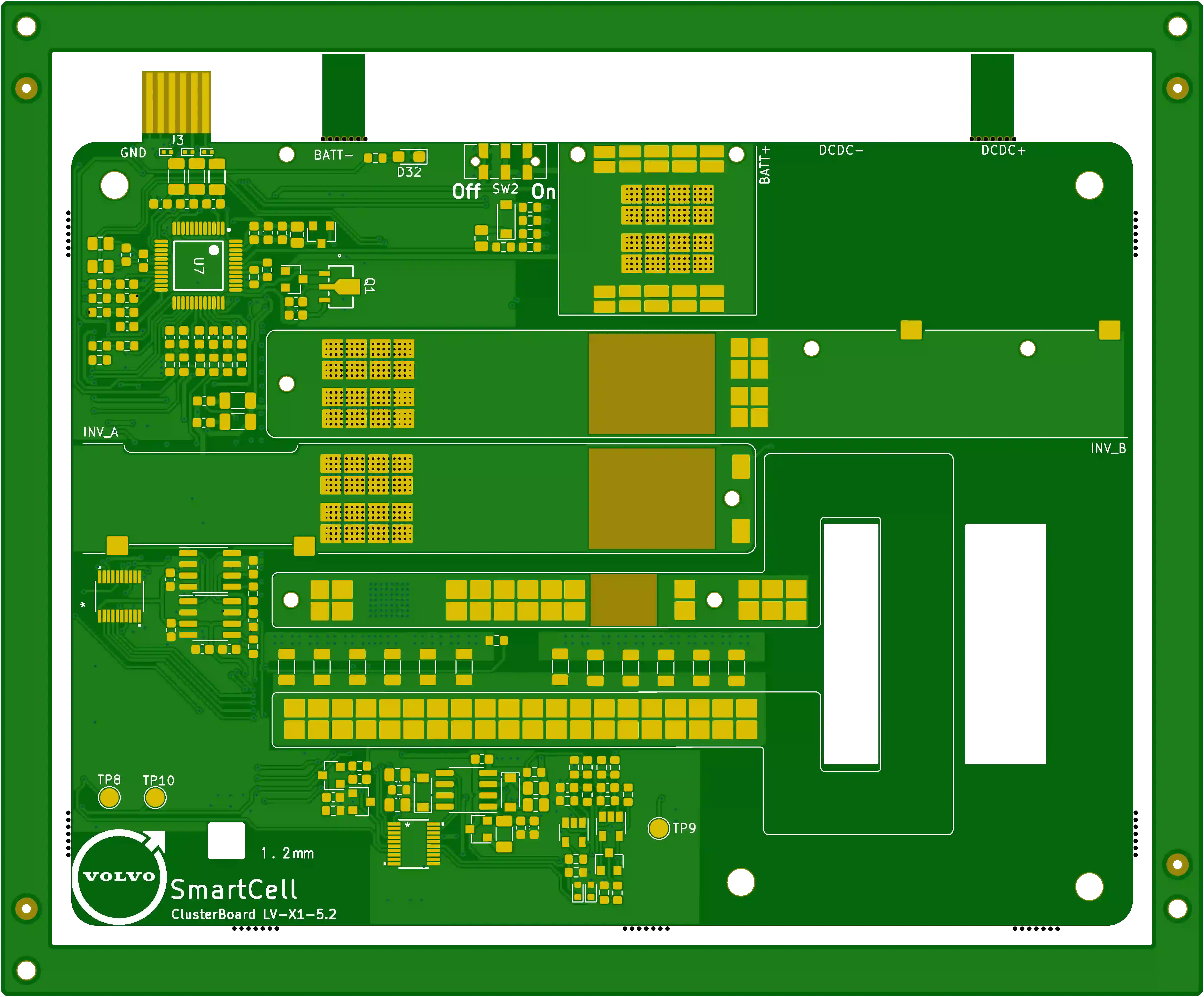
Evaluating 1.2mm Thickness Control and Depth Drill Precision in 4-Layer FR4 Production
This case evaluates the manufacturability of a 4-layer FR4 PCB with tight 1.2mm ±0.12mm thickness tolerance, 0.78mm controlled-depth drilling for L2/L3 pad exposure, and blind vias. This engineering capability assessment details lamination control, depth drill precision, and process validation for reliable production.
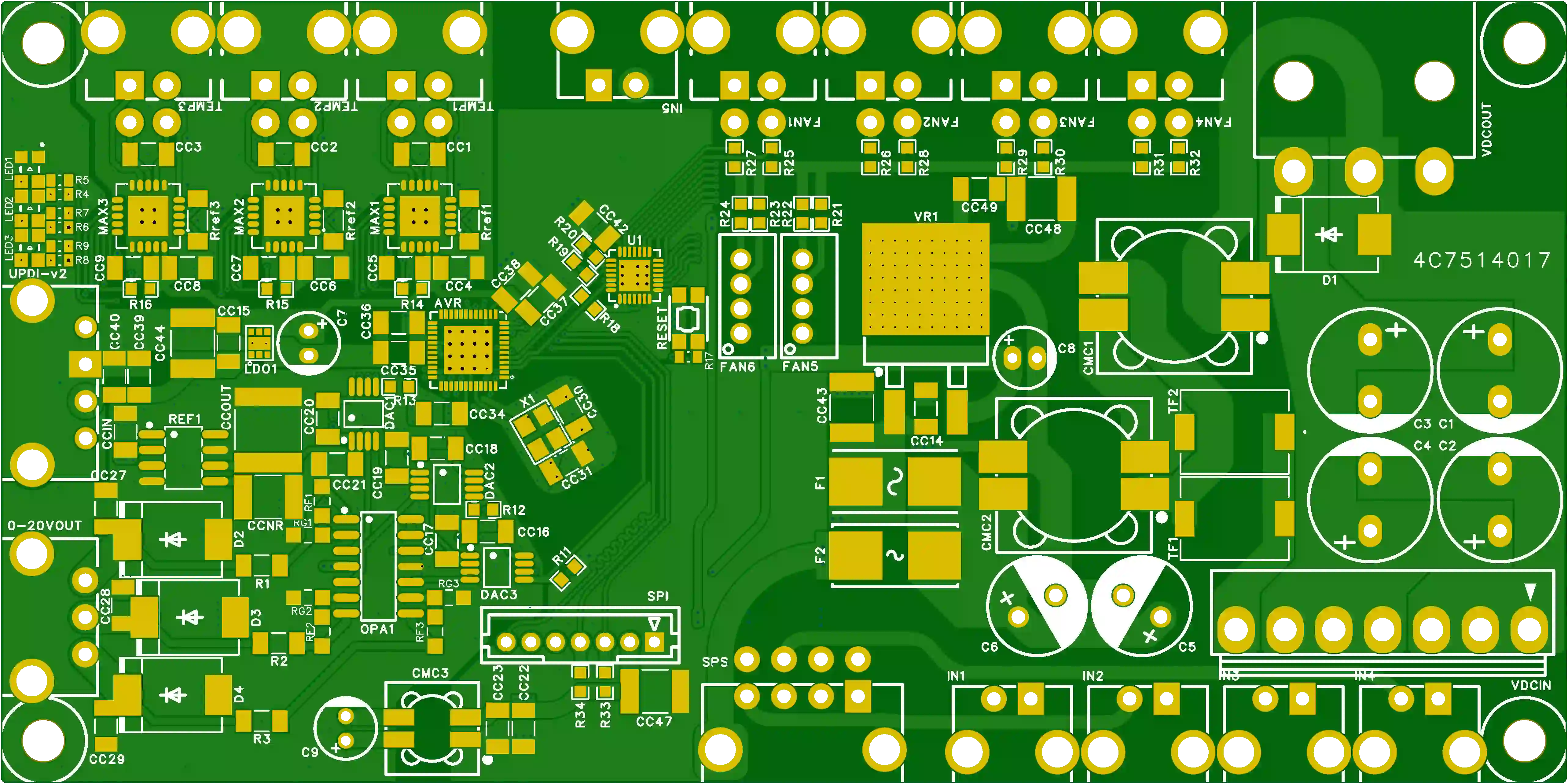
How Conflicting Via Data and Soldermask Definitions Triggered CAM Review in a 4-Layer HDI PCB
As Senior CAM Auditor at AIVON, I investigated conflicting blind via sizes, soldermask vs SMT data, and plugging requirements in a 4-layer FR-4 HDI PCB. Discover how targeted Engineering Questions resolved data-to-manufacturing conflicts, ensured stackup accuracy, and prevented production risks before fabrication. Essential insights for designers on HDI via processing and CAM verification.


