


PCB Application
Printed circuit boards (PCBs) form the backbone of modern electronics, enabling the seamless integration of components in devices ranging from smartphones to industrial machinery. In the PCB Application category, we delve into the diverse ways these essential components are deployed across industries, offering a comprehensive resource for engineers, designers, and enthusiasts seeking to understand and implement effective solutions. This category explores the practical implementation of PCBs in real-world scenarios, from consumer electronics and automotive systems to medical devices and renewable energy technologies. Readers will find detailed discussions on how PCB designs influence performance, reliability, and efficiency in applications such as IoT devices, where compact layouts support wireless connectivity, or in aerospace engineering, where robust PCBs withstand extreme conditions. By examining these examples, professionals can gain insights into optimizing board layouts for specific environments, reducing failure rates, and enhancing overall system functionality. Our collection includes in-depth guides that walk through application-specific design considerations, step-by-step tutorials on prototyping for emerging technologies like electric vehicles, and expert insights into best practices for signal integrity and thermal management. Whether you are troubleshooting common issues in high-frequency applications or exploring innovative uses in wearable tech, the articles here provide actionable knowledge grounded in current industry standards. As you navigate through these resources, you will uncover strategies to adapt PCB applications to evolving demands, ensuring your projects remain at the forefront of technological advancement. With a focus on technical relevance, this category bridges theoretical concepts with hands-on implementation, empowering you to apply proven techniques in your own work. Delving into multiple pieces within PCB Application equips you with a broader perspective, fostering innovation and problem-solving in electronics design.
Latest Blogs

Network Switch PCB Layout: A Comprehensive Design-to-Production Guide
Master network switch PCB layout design for high performance and reliability, covering guidelines, manufacturing, SMT assembly, and through-hole technology.
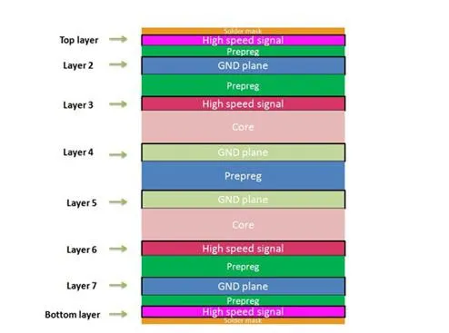
Designing 8-Layer PCBs for High-Current and High-Voltage Power Electronics
Discover expert PCB design for power electronics using 8-layer boards optimized for demanding high-current and high-voltage applications. Learn key considerations for trace sizing, creepage, layer stackup, and manufacturing to minimize noise, heat, and risk while maximizing performance.

6 Layer PCB Stackup: Standard Configurations, Examples, and Thickness
Explore a 6 layer PCB stackup with practical examples, standard layer arrangements, board thickness options, and design tips for power distribution, signal integrity, and high-current applications.

Telecommunications PCB Assembly: From Prototyping to Mass Production
Master telecommunications PCB assembly: Transition from prototyping to mass production with SMT and through-hole techniques. Optimize yields, reduce defects, and ensure signal integrity per IPC standards—essential for 5G routers and switches.
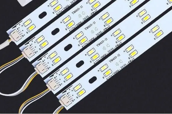
Cost-Effective Brilliance: Optimizing LED Lighting PCB Design for Mass Production
Unlock cost-effective LED lighting PCBs: Explore minimizing material costs, automated assembly, panelization optimization, and DFM best practices. Reduce expenses in mass production while ensuring reliability per IPC standards—ideal for high-volume designs.
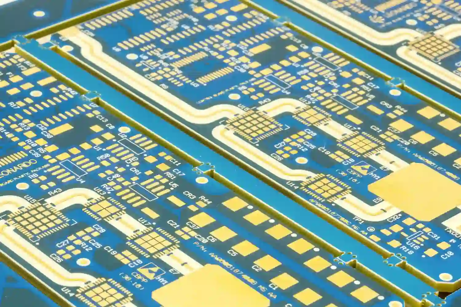
Selecting the Right PCB Laminate for High-Frequency Ultrasound Applications
Discover how to select the right PCB laminate for high-frequency ultrasound applications. Compare RO4350B, PTFE, Megtron 7 and LCP on Df, Dk, and signal integrity at 50–100 MHz. Practical design guidelines for superior imaging depth and SNR.
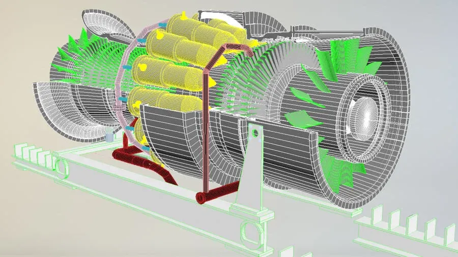
Using Heavy Copper PCBs for High-Power Industrial Sensors
Discover how heavy copper PCBs deliver reliable 100A+ power distribution and superior thermal management in harsh industrial sensors. Includes design steps, troubleshooting tables, steel-mill case study, and IPC-compliant best practices for 2026 Industry 4.0 deployments.

Heavy Copper PCBs: Powering High-Demand Aircraft Cockpit Displays
Explore heavy copper PCBs for high-demand aircraft cockpit displays, optimizing power layer design and thermal management in power PCBs to meet aerospace power requirements. Learn assembly best practices, DO-160 compliance, and 2025 trends for reliable high current PCBs—enhance efficiency in avionics.
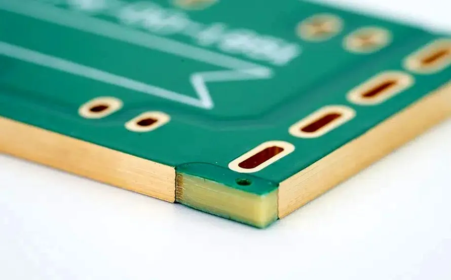
Heavy Copper Handling: Designing PCBs for High-Power Industrial Applications
Learn key heavy copper PCB design rules for high-power electronics. This guide covers IPC-2152 current capacity, thermal management, and mechanical reliability for industrial applications.

Flexible PCB for Medical Wearable Devices: Design & Applications
Learn how flexible PCB for wearable devices supports compact, lightweight electronics, medical wearables, and consumer products, with key design and material considerations.
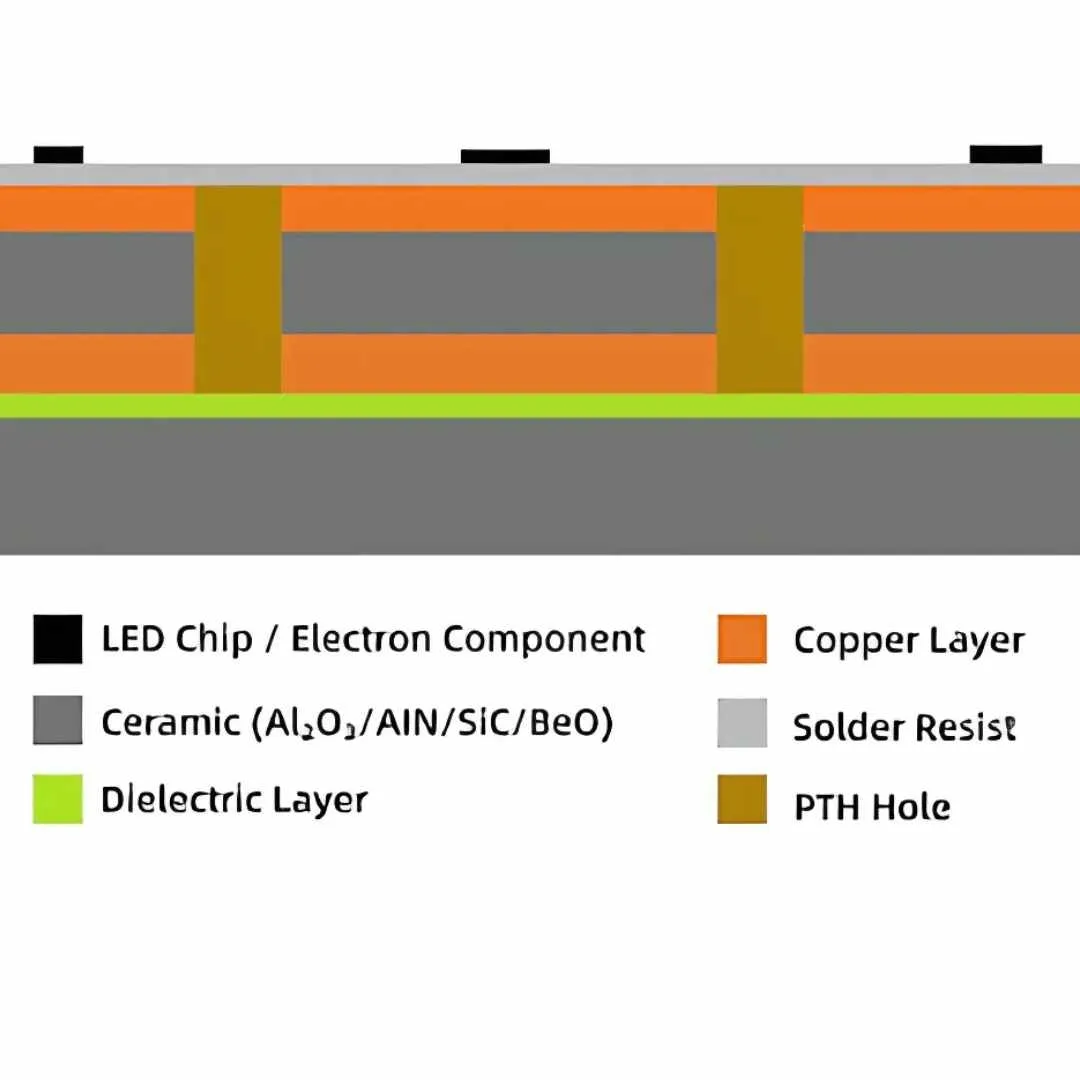
Beyond Aluminum: Exploring Advanced Materials for High-Power LED PCBs
Explore advanced MCPCB materials for high-power LEDs. Compare ceramic, copper core, and IMS substrates on thermal conductivity, cost, and high-temperature performance.
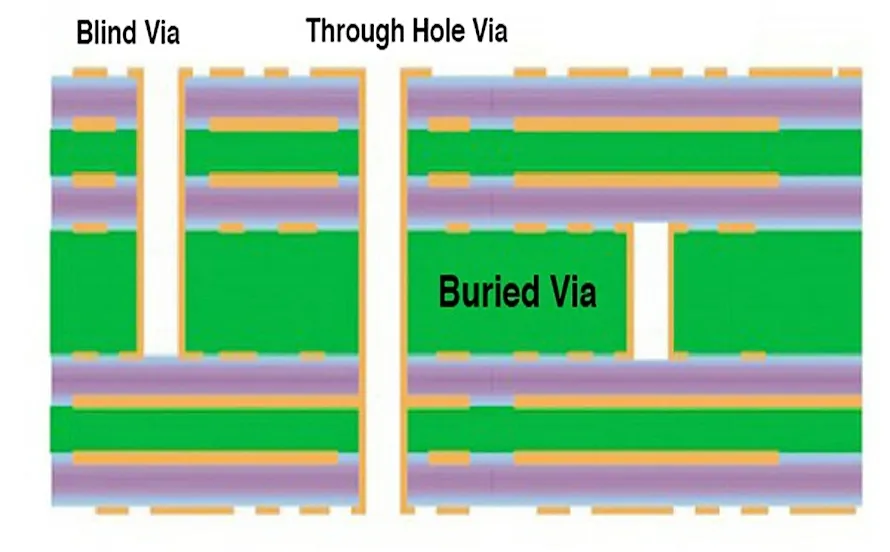
The Art of Blind and Buried Vias in High-Density Ultrasound PCBs
An engineer's guide to blind and buried vias in ultrasound PCBs. Covers laser drilling, via-in-pad, and best practices for high-density interconnect (HDI) reliability.


