In production, multilayer pcb assembly is handled by locking the stackup, copper distribution, and surface finish early in CAM so the board that leaves the fab line can actually be reflowed without constant profile tweaks. What we typically see on the CAM side is copper imbalance across the panel, via-in-pad under large thermal pads, and layer counts that create local thermal mass differences. Most factories will flag these during the first DFM pass and either require design changes or apply specific process compensations before the boards reach the SMT line. Flatness is checked at the finished board stage, and surface finish is selected to match the expected reflow window rather than left as a default.
From a fabrication standpoint, this becomes sensitive because the multilayer structure is already fixed by the time the boards arrive for assembly. The same copper planes and dielectric thicknesses that give the electrical performance also determine how heat moves during reflow. Component placement relative to those planes is not just a layout choice; it directly changes local heat sinking and therefore the window for reliable joints.

Where copper plane density starts to control the reflow window
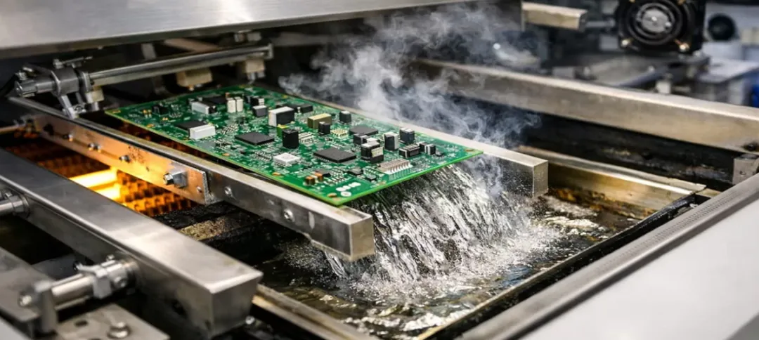
In production, this usually shows up as incomplete solder fillets or voiding on components sitting over heavy copper planes while nearby parts on lighter copper reach liquidus without trouble. The root cause sits in the lamination and plating steps. Multiple power and ground planes, especially when they are not balanced left-to-right or top-to-bottom, create local differences in thermal mass that the reflow oven cannot fully equalize. Equipment tolerance on oven zone control is typically ±2–3 °C, but a solid 2 oz plane under a pad can pull heat away fast enough that the joint never reaches the full liquidus time even when the profile looks correct on a bare board thermocouple.
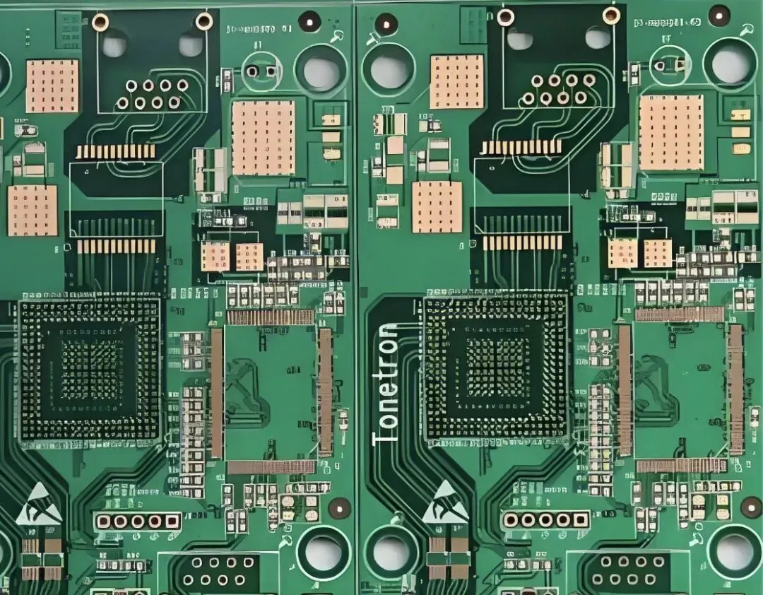
Panelization constraints make it worse. We rarely run single boards; we run panels, and copper balance across the panel is required for lamination flatness. When the designer places large planes only under certain areas of the circuit, the CAM engineer still has to fill the panel borders and rails to keep the stack flat. Those added copper areas then act as additional heat sinks once the panel is broken out or when boards are run in panel form through the oven. Registration accuracy between layers is typically held to ±75 µm or better on modern equipment, but that does not change the fact that a via barrel or plane connection still conducts heat differently than open dielectric.
Material behavior in the process flow adds another layer. Prepreg resin content and glass weave affect both dielectric thickness and how heat spreads laterally. Thicker boards (1.6 mm and above with high layer counts) simply take longer to bring the center of the panel up to temperature, so the top-side components see a different thermal history than bottom-side parts if the oven is not run with a longer soak.
What shows up on the SMT line when thermal mass is left uncontrolled
Yield drop is the first thing we measure. Boards with large copper planes under fine-pitch packages routinely show 3–8 % higher void rates on X-ray compared with the same parts on lighter copper. Incomplete joints appear as insufficient wetting on thermal pads, which then fail electrical test or show up as intermittent opens after thermal cycling. Misalignment of components is less common but does occur when warpage exceeds 0.75 % of the board diagonal; the panel bows during the peak reflow zone and the placement machine's earlier alignment no longer matches the actual pad location.
Solder mask shift is rarely the direct cause, but when mask openings are tight over via-in-pad, any residual resin or incomplete plugging lets solder wick down the via and starve the joint. Assembly failure then appears as lifted pads or cracked joints during rework, because the operator has to apply extra heat to clear the voided area. Rework and scrap become the practical result: boards that fail AOI or X-ray go to a manual station, and a multilayer board with buried vias is not something you want to heat more than once or twice. Shipment delays follow when the line has to stop for profile optimization or when a whole panel lot is held for flatness re-measurement.

How factories compensate for copper density and via structure before the boards reach the oven
Most factories will handle this by adjusting the CAM output and the process recipe together. On the CAM side we add thermal reliefs or hatching on internal planes under large pads when the design allows it; the reliefs are typically 0.2–0.3 mm wide spokes so electrical performance stays acceptable while thermal mass drops. For via-in-pad we require epoxy fill and planarization, or at least copper cap plating, so solder cannot wick. The fill is checked by microsection on a first-article coupon because incomplete fill is the most common source of voids later. Panel design strategies include keeping copper balance within 10–15 % across the panel area and adding thieving only outside the circuit outline so the rails do not sit under component fields.
Process parameter control focuses on the reflow profile. We run a longer soak (typically 60–90 s between 150–180 °C) on boards thicker than 1.6 mm or with more than six layers of 1 oz or heavier copper. Peak temperature is kept at the lower end of the paste window (usually 235–245 °C for SAC305) to avoid damaging the board while still giving the heavy copper areas enough time above liquidus. Inspection methods include both AOI for placement and X-ray for thermal pads; the X-ray criteria are tightened to less than 25 % void area on power pads when the design has solid planes. Alignment is verified by placing fiducials on both sides and confirming the panel remains within 0.1 mm flatness after reflow on a sample basis.
Surface finish selection is part of the same decision. ENIG is preferred when the board will see multiple reflow passes or when fine-pitch parts sit over planes, because the nickel barrier reduces copper dissolution and the gold gives a consistent wetting surface. HASL is still used on lower-density boards where the extra copper from the coating does not create additional thermal mass problems. We usually flag this during DFM review when the design shows mixed surface-finish requirements or when the assembly house has already locked a paste and profile that only works with one finish.
Component density is managed by spacing rules that come from the placement machine and the rework station, not only from the designer's DRC. We typically require 0.3 mm minimum clearance between fine-pitch packages and adjacent discretes so the nozzle can pick and the AOI can see the joints. Test points are kept on the outer layers and away from dense areas so in-circuit test probes do not compete with component bodies. These rules are applied because high-density multilayer boards already have limited real estate; once the parts are placed, inspection and rework access become the yield limiters.

When the factory will accept a looser thermal or density condition
Relaxation is allowed on prototype or low-volume runs where the customer accepts a higher void percentage or a custom reflow profile. Designs with mostly 1 oz copper, balanced stackups, and no via-in-pad under thermal pads can often run on the standard oven recipe without extra soak time. The trade-off is yield and consistency: the same board that passes on a short prototype lot may show higher fallout once it moves to a production panel size and a fixed profile. High-density boards that still need the solid planes for electrical reasons are left with the tighter controls; we do not relax those because the rework cost on a multilayer with buried features quickly exceeds the cost of the original process adjustments.
Where fab and assembly limits finally meet on multilayer boards
Multilayer pcb assembly holds together when the copper balance, via fill, and finished flatness are treated as process limits that both the fab and the SMT line already own. The numbers we hold—copper balance inside 10–15 %, void area under 25 % on power pads, flatness inside 0.1 mm after reflow—come from the lamination press, the plating line, and the oven zones that are already running. Designs that ignore those limits simply move the yield loss from the fab shop to the assembly floor, where rework on buried vias is slower and more expensive. The practical path is to lock the stackup and plane strategy in CAM before the first panel is pressed, then confirm the same board on the oven with a first-article X-ray rather than discovering the thermal mismatch after the full lot is built.
FAQ
Q1: Can we run the same reflow profile on an 8-layer board that we use on a 4-layer board?
A1: Only if the copper weight and plane coverage stay similar. An 8-layer stack with multiple 2 oz planes needs a longer soak; the extra layers add thermal mass that a 4-layer profile never sees. We measure it with thermocouples on the actual panel, not on a bare coupon.
Q2: Does ENIG change the void rate under a large thermal pad?
A2: It improves wetting consistency, but it does not remove the voids caused by solid copper underneath. The nickel barrier keeps the copper from dissolving, yet the heat sink effect of the plane remains. Hatching or reliefs still do more for void reduction than the finish alone.
Q3: How much warpage is still acceptable once the board is fully populated?
A3: We hold finished flatness to 0.75 % of the diagonal before placement and re-check a sample after reflow. Beyond that the placement machine's vision system and the later AOI start to disagree on pad location, and fine-pitch parts show opens that were not present at first placement.
Q4: Can test points sit on internal layers if we use plated through-holes?
A4: They can electrically, but the probe access and the risk of damaging buried features during ICT make it impractical on high-density multilayer boards. We keep test points on the outer layers and clear of component bodies so the fixture can land without hitting parts or vias that have already been filled.
Q5: What happens if copper thieving is placed under a component field instead of in the rails?
A5: The extra copper becomes another heat sink during reflow and can create local voiding or incomplete fillets on nearby parts. We keep thieving outside the circuit outline so it balances the panel for lamination without affecting the thermal profile of the populated area.